Schematics
Introduction
Lcapy can generate high quality schematics from a netlist using the Circuitikz LaTeX package. This is much easier than writing Circuitikz commands directly in LaTeX. For the fastest way to generate a schematic from a netlist, see schtex. For a graphical user interface, see https://github.com/mph-/lcapy-gui.
A semi-automatic component placement is used with hints required to designate component orientation and explicit wires to link nodes of the same potential but with different coordinates.
Here’s an example:
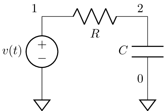
>>> cct = Circuit("""
... V 1 0 {v(t)}; down
... R 1 2; right=2, i=i(t)
... C 2 0_2; down, v=v_C(t)
... W 0 0_2; right
... ; draw_nodes=connections, label_ids=false, label_nodes=none""")
>>> cct.draw()
Note, the orientation hints are appended to the netlist strings with a semicolon delimiter. The drawing direction is with respect to the first node. The component W is a wire. Node names starting with an underscore are not shown.
The image generated by this netlist is:

Here’s an example with implicit ground connections added automatically:
>>> cct = Circuit("""
... V 1 0 {v(t)}; down
... R 1 2; right=1.5
... C 2 0; down
... ; autoground=true, label_ids=false, draw_nodes=connections""")
>>> cct.draw()
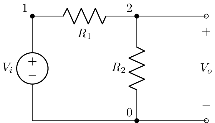
Here’s another example, this time loading the netlist from a file and saving the created schematic as a PDF file:
>>> from lcapy import Circuit
>>> cct = Circuit('voltage-divider.sch')
>>> cct.draw('voltage-divider.pdf')
Here are the contents of the file ‘voltage-divider.sch’:
Vi 1 0_1; down
R1 1 2; right=1.5
R2 2 0; down
P1 2_2 0_2; down, v=V_o
W 2 2_2; right
W 0_1 0; right
W 0 0_2; right
Here, P1 defines a port. This is shown as a pair of open blobs. The wires do not need unique names.
Most aspects of the schematic are configurable, such as the component style, size, spacing, and color. Compare the following schematic with the one above.
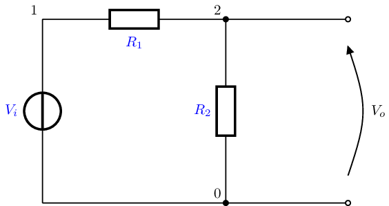
These two schematics use the same netlist but the second one has the following configuration line:
; draw_nodes=connections, node_spacing=3, scale=0.5, style=european, bipole label style={color=blue}
Netlists
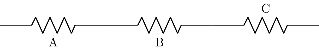
Schematics are described using the same netlist syntax as used for circuit analysis. See Component specification for a list of known components. The drawing attributes (see Attributes) are specified after a semicolon delimiter. For example:
R1 1 2; right=2, color=blue
This defines a resistor between nodes 1 and 2 drawn in blue to the right with length 2.
Component orientation
Lcapy uses a semi-automated component layout. Each component requires a specified orientation: up, down, left, right. In addition, attributes can be added to override color, size, etc.
The drawing direction provides a constraint. For example, the nodes of components with a vertical orientation have the same x coordinate, whereas nodes of horizontal components have the same y coordinate.
The component orientation can be specified by a direction attribute. Note, this rotates the component:
right (0 degrees)
left (180 degrees)
up (90 degrees)
down (-90 degrees)
For example:
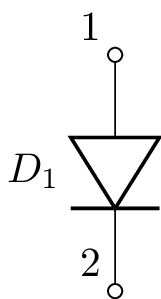
D1 1 2;right
D1 1 2;down
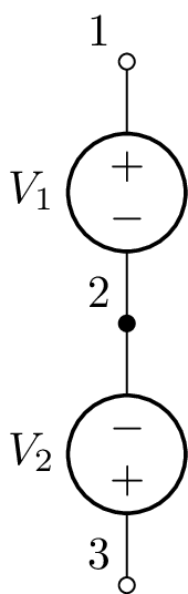
Note, the drawing direction is from the positive node to the negative node. For example,
V1 1 2; down
V2 3 2; up
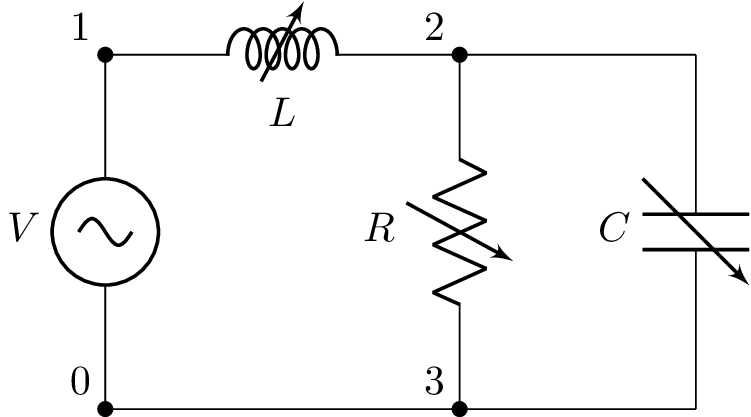
The component orientation is also specified by a rotation angle. This angle is degrees anticlockwise with zero degrees being along the positive x axis. For example,
>>> cct.add('D1 1 2; rotate=45')
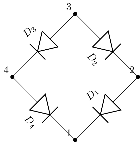
Here’s an example of how to draw a diode bridge:
D1 2 1; rotate=225, size=1.5
D2 3 2; rotate=-45, size=1.5
D3 3 4; rotate=225, size=1.5
D4 4 1; rotate=-45, size=1.5
Most components can be mirrored about the x-axis using the mirror or flipud attributes and mirrored about the y axis with the invert or fliplr attribute. For example, to switch the order of the inverting and non-inverting inputs of an opamp use:
>>> cct.add('E1 1 2 opamp 3 0; right, mirror')
Note, the mirroring is performed before rotations are applied. Opamps also have a mirrorinputs option that switches the inverting and non-inverting inputs without mirroring the entire component.
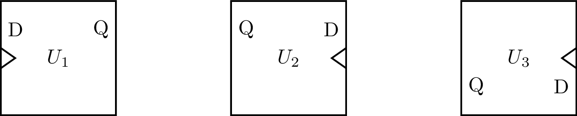
Here’s an example of using invert to mirror a D flip-flop in the y-axis, compared to rotating the flip-flop:
U1 dff;
U2 dff; fliplr
U3 dff; left
O U1.mid U2.mid; right=2
O U2.mid U3.mid; right=2
Component size
By default each component has a minimum size of 1. This can be stretched to satisfy a node constraint. The minimum size is specified using the size attribute, for example:
>>> cct.add('R1 1 2; right, size=2')
The size argument is used as a scale factor for the component node spacing. The size can also be specified by adding a value to the left, right, up, or down arguments. For example:
>>> cct.add('R1 1 2; right=2')
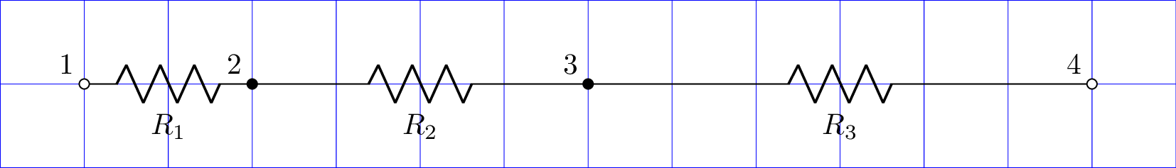
Here’s a comparison of resistors of different sizes.
R1 1 2; right
R2 2 3; right=2
R3 3 4; right=3
;help_lines=1
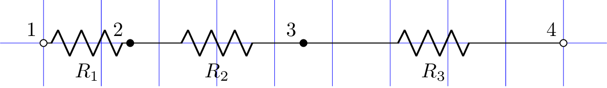
By default, a component with size 1 has its nodes spaced by 2 units. This can be changed using the node_spacing option of the schematic. For example,
R1 1 2; right
R2 2 3; right=2
R3 3 4; right=3
;node_spacing=1.5, help_lines=1
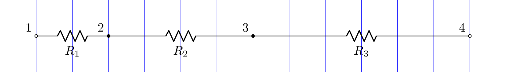
Be default, a component has a length of 1.5 units. This can be changed using the cpt_size option of the schematic. For example,
R1 1 2; right
R2 2 3; right=2
R3 3 4; right=3
;cpt_size=1, help_lines=1
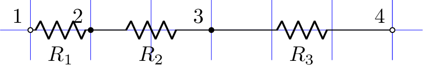
R1 1 2; right
R2 2 3; right=2
R3 3 4; right=3
;cpt_size=1, node_spacing=1, help_lines=1
The size of components can scaled with the scale attribute:
R1 1 2; right
R2 2 3; right=2, scale=2
R3 3 4; right=3, scale=3
;help_lines=1
The overall schematic can be scaled with the scale option of the schematic:
R1 1 2; right
R2 2 3; right=2
R3 3 4; right=3
;scale=0.5, help_lines=1
Nodes
Nodes are shown by a blob. By default, only the primary nodes (those not starting with an underscore) are shown by default. This is equivalent to:
>>> cct.draw(draw_nodes='primary')
All nodes can be drawn using:
>>> cct.draw(draw_nodes='all')
Only the nodes where there are more than two branches can be drawn using:
>>> cct.draw(draw_nodes='connections')
No nodes can be drawn using:
>>> cct.draw(draw_nodes=False)
By default, only the primary nodes are labelled. All nodes can be labelled (this is useful for debugging) using:
>>> cct.draw(label_nodes='all')
No nodes can be labelled using:
>>> cct.draw(label_nodes=False)
Only nodes starting with a letter can be labelled using:
>>> cct.draw(label_nodes='alpha')
In this case nodes with names such as in and out will be displayed but not numeric node names.
These options can be stored with the schematic netlist, for example:
C1 1 0 100e-12; down, size=1.5, v={5\,kV}
R1 1 6 1500; right
R2 2 4 1e12; down
C2 3 5 5e-9; down
W 2 3; right
W 0 4; right
W 4 5; right
SW 6 2 no; right=1.5, l=
; draw_nodes=connections, label_nodes=False, label_ids=False
Node names
Circuit nodes are usually identified by a number. They can be given arbitrary names provided they do not contain a period (.). By default, nodes with names starting with an underscore are not drawn. The name can contain an underscore to denote a subscript or a caret to denote a superscript. For example, T_123.
Node names starting with a period are a short-hand notation. For example:
R1 1 .2; right
C1 R1.2 3; right
is short-hand for:
R1 1 R1.2; right
C1 R1.2 3; right
Node names not starting with an underscore are considered primary nodes. Node names starting with an underscore are considered secondary nodes (usually they are at the same potential as a primary node and do not need to be labelled). For backward compatibility, nodes with names that contain an underscore and start with a digit are considered secondary.
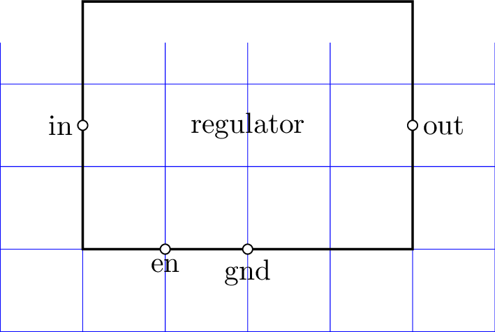
Node names can also refer to pins of Shape and Chip components. For example:
U1 regulator; right
W  1 U1.in; right
W  U1.gnd 0; down
Components
Only linear, time-invariant, components can be analyzed by Lcapy. For a list of these, see Component specification. However, many others can be drawn.
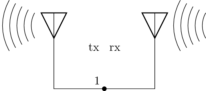
Antennas
ANT1 1; left, kind=tx, mirror, l=tx
ANT2 1; right, kind=rx, l=rx
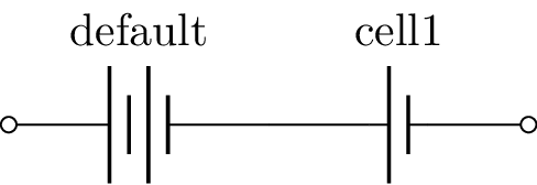
Batteries
BAT1 1 2; right, l=default
BAT2 2 3; right, kind=cell1, l=cell1
; label_nodes=false, draw_nodes=connections
Blocks
BL1 1 2; right, kind=vco, l=vco
BL2 2 3; right, kind=highpass, l=highpass
BL3 3 4; right, kind=lowpass, l=lowpass
BL4 4 5; right, kind=bandpass, l=bandpass
BL5 5 6; right, kind=highpass2, l=highpass2
BL6 6 7; right, kind=lowpass2, l=lowpass2
BL7 7 8; right, kind=amp, l=amp
BL8 8 9; right, kind=dcdc, l=dcdc
BL9 9 10; right, kind=dcac, l=dcac
BL10 10 11; right, kind=acdc, l=acdc
BL11 11 12; right, kind=twoportsplit, l=twoportsplit
; label_nodes=false, draw_nodes=connections

BL1 1 2; right, kind=adc, l=adc
BL2 2 3; right, kind=dac, l=dac
BL3 3 4; right, kind=piattenuator, l=piattenuator
BL4 4 5; right, kind=vpiattenuator, l=vpiattenuator
BL5 5 6; right, kind=tattenuator, l=tattenuator
BL6 6 7; right, kind=vtattenuator, l=vtattenuator
BL7 7 8; right, kind=phaseshifter, l=phaseshifter
BL8 8 9; right, kind=vphaseshifter, l=vphaseshifter
BL9 9 10; right, kind=dsp, l=dsp
BL10 10 11; right, kind=fft, l=fft
BL11 11 12; right, kind=twoport, l=twoport
; label_nodes=false, draw_nodes=connections

Note, the block names match those used by Circuitikz.
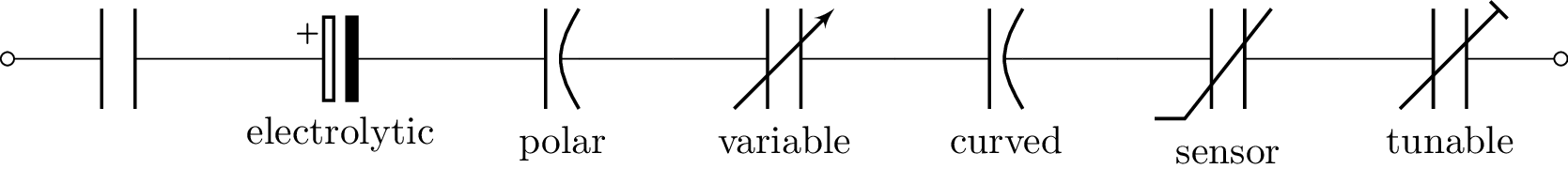
Capacitors
C1 1 2; right, l=
C2 2 3; right, kind=electrolytic, l=electrolytic
C3 3 4; right, kind=polar, l=polar
C4 4 5; right, kind=variable, l=variable
C5 5 6; right, kind=curved, l=curved
C6 6 7; right, kind=sensor, l=sensor
C7 7 8; right, kind=tunable, l=tunable
; label_nodes=false, draw_nodes=connections
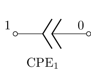
Constant phase elements (CPE)
CPE1 1 0; right
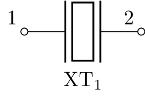
Crystals
XT1 1 2; right
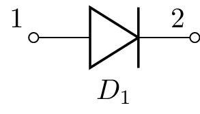
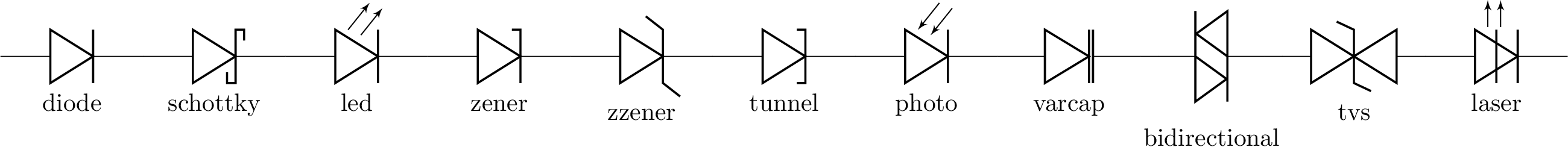
Diodes
Diodes can be drawn but not simulated. A standard diode is described using:
Dname Np Nm
Different kinds of diodes can be specified by the kind option, for example,
D1 1 2; right, l=diode
D2 2 3; right, kind=schottky, l=schottky
D3 3 4; right, kind=led, l=led
D4 4 5; right, kind=zener, l=zener
D5 5 6; right, kind=zzener, l=zzener
D6 6 7; right, kind=tunnel, l=tunnel
D7 7 8; right, kind=photo, l=photo
D8 8 9; right, kind=varcap, l=varcap
D9 9 10; right, kind=bidirectional, l=bidirectional
D10 10 11; right, kind=tvs, l=tvs
D11 11 12; right, kind=laser, l=laser
; draw_nodes=none, label_nodes=none
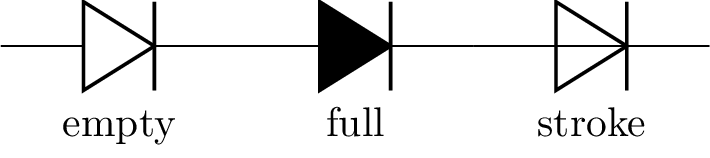
The drawn style is controlled by the style option, for example,
D1 1 2; right, l=empty
D2 2 3; right, style=full, l=full
D3 3 4; right, style=stroke, l=stroke
; draw_nodes=none, label_nodes=none
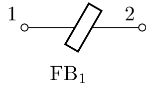
Ferrite beads
FB1 1 2; right
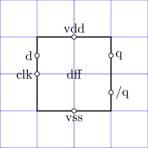
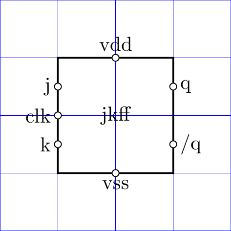
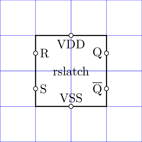
Flip-flops and latches
The syntax is:
Uname dff|jkff|rslatch
Gyrators
GY1 1 2 3 4 R; right
Inductors and chokes
L1 1 2; right, l=
L2 2 3; right, kind=variable, l=variable
L3 3 4; right, kind=tunable, l=tunable
L4 4 5; right, kind=sensor, l=sensor
L5 5 6; right, kind=choke, l=choke
L6 6 7; right, kind=twolineschoke, l=twolineschoke
L7 7 8; right, kind=american, l=american
L8 8 9; right, kind=european, l=european
; label_nodes=false, draw_nodes=connections

Integrated circuits
ICs can be drawn but not simulated. Here’s an example:
; draw_nodes=connections, help_lines=1
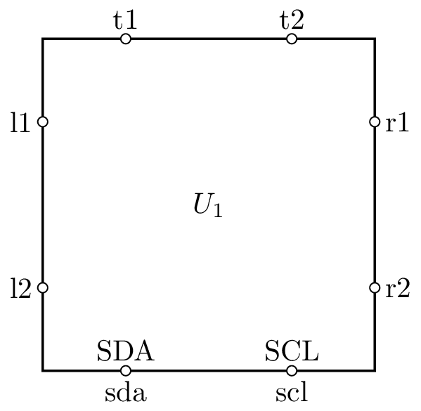
U1 chip2121; right=2, l={MCU}, pinlabels={r1=PIO1,r2=PIO2}
W U1.vdd VDD; up=0.2, implicit, l=3V3
W U1.vss 0; down=0.7, 0V
R1 U1.r2 1; right
D1 1 3 led; down
W 3 0; down=0.1, 0V
R2 U1.r1 2; right
W 2 5; right
D2 5 4 led; down
W 4 0; down=0.1, 0V
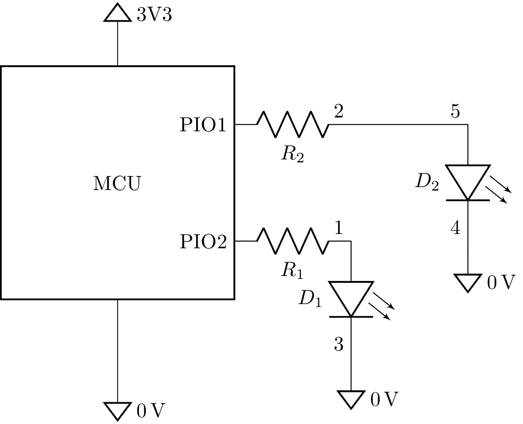
In this example, the chip2121 keyword specifies a block with two pins on the left, one on the bottom, two on the right, and one at the top. The component has pre-defined pinnames, l1, l2, vss, r2, r1, and vdd; these can be modified. Since the pin names start with a dot the associated node names are prefixed by the name of the chip, for example, U1.out1.
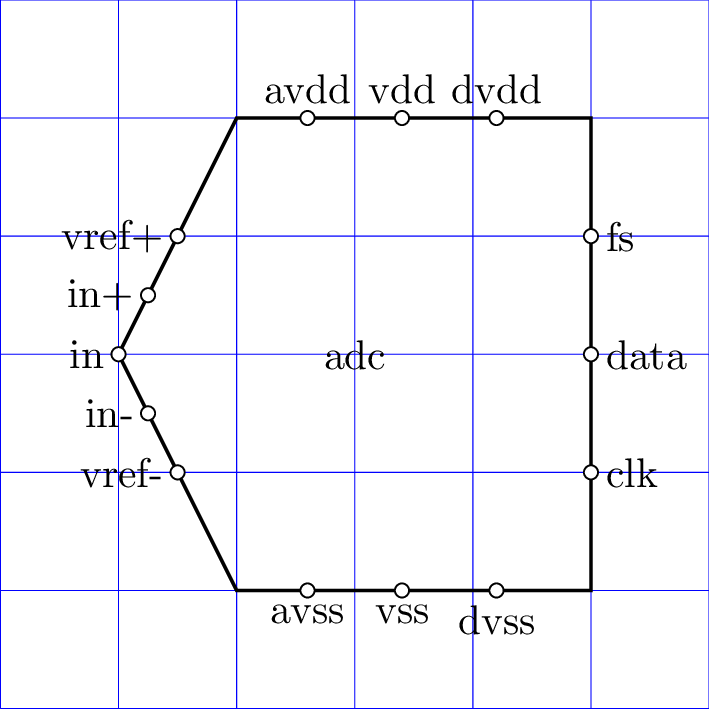
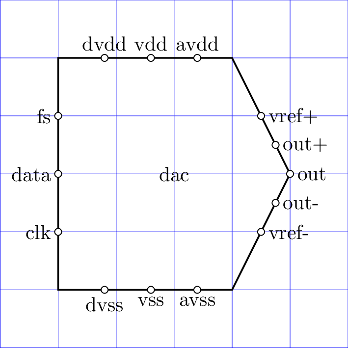
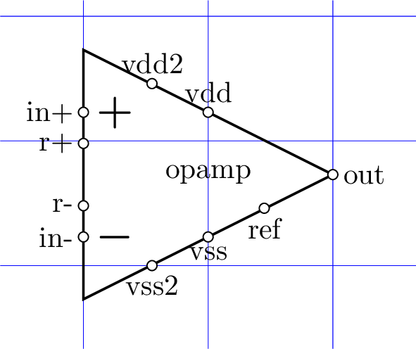
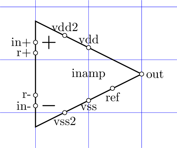
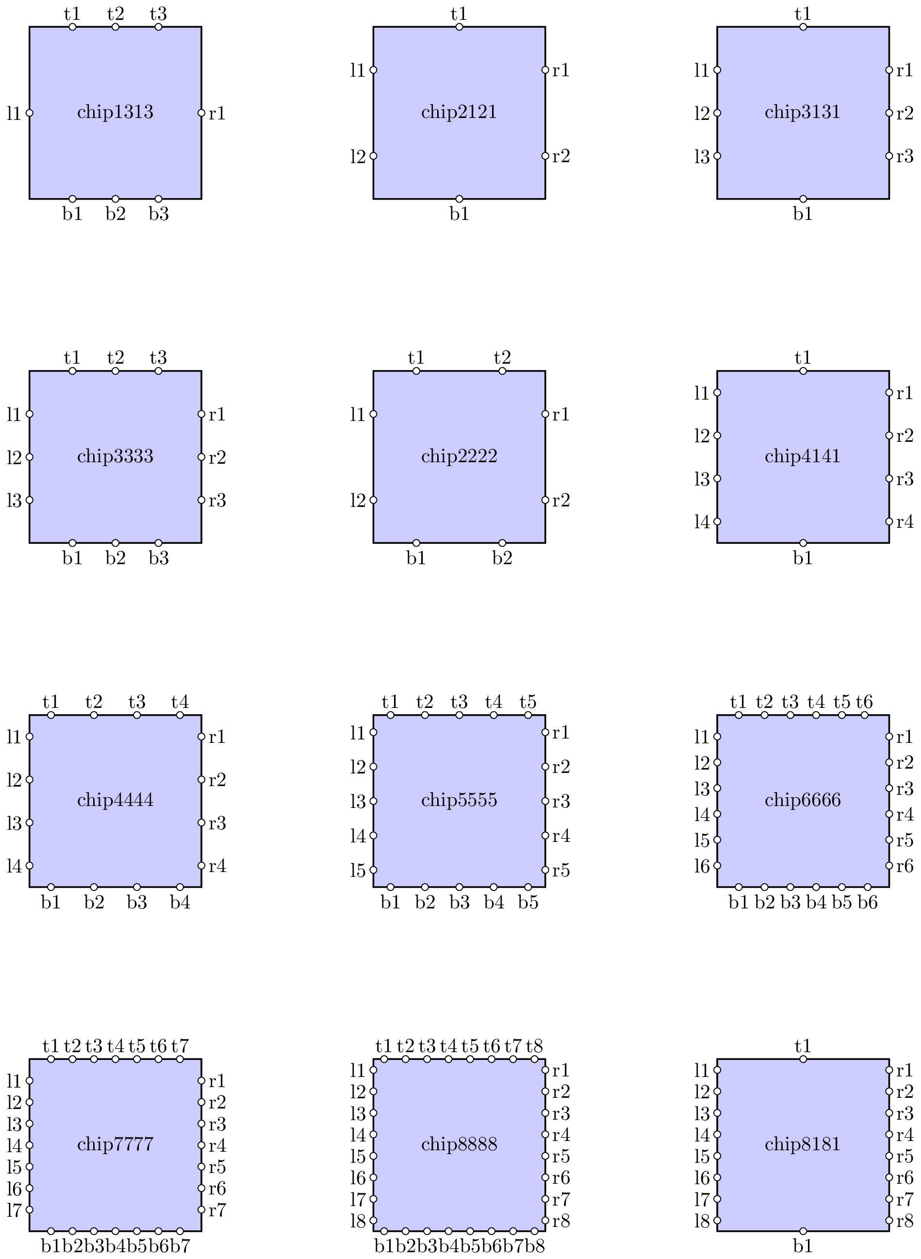
- The supported chips are:
chip1313
chip2121
chip2222
chip3131
chip3333
chip4141
chip4444
chip5555
chip6666
chip7777
chip8181
chip8888
buffer
inverter
regulator
adc
dac
fdopamp
inamp
isoamp
opamp
diffdriver
diffamp
Chips are subclassed from the Shape class and thus the pins can be labelled, renamed, etc. For example:
U1 chip2222; right, pindefs={sda=b1,scl=b2}, pinlabels={sda=SDA,scl=SCL}, pinnodes=all, pinnames=all
Here is a gallery of some of the chips. Note, the aspect ratio can be changed with the aspect attribute.
Logic gates
Logic gate support is preliminary and the gates may change in size. The syntax is:
Uname and|or|xor|nand|nor|xnor

IEEE standard shapes are used.
Meters
Here’s an example using a voltmeter and an ammeter:
BAT 1 0 7.2; down=1.5, l={7.2\,V}
AM 1 2; right=1.5
R 2 3; down
W 0 3; right
W 2 2_1; right
W 3 3_1; right
VM 2_1 3_1; down

Miscellaneous components
Miscellaneous Circuitikz bipole components can be drawn using a MISC component. For example,
MISC1 1 2; right, kind=thermistor, l=thermistor
MISC2 2 3; right, kind=memristor, l=memristor
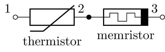
See the Circuitikz manual for bipole components that can be drawn.
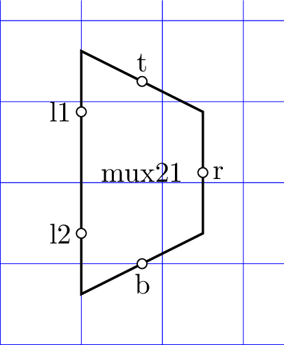
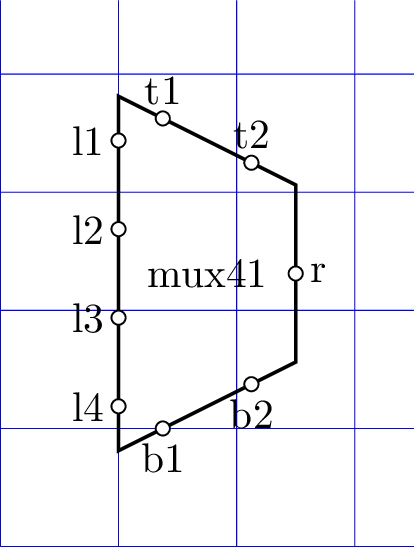
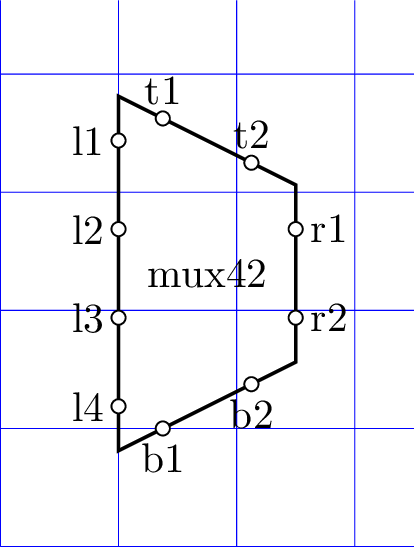
Multiplexers
The syntax is:
Uname mux21|mux41|mux42
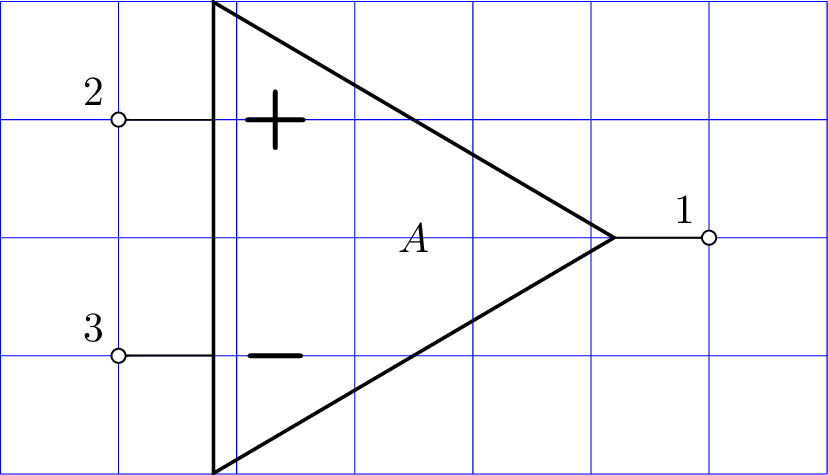
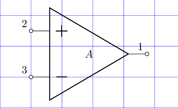
Opamps
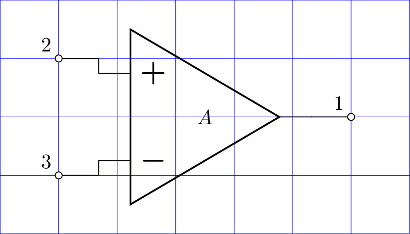
Opamps can be drawn using the opamp argument to a VCCS. For example:
E 1 0 opamp 2 3 A; right
;help_lines=1
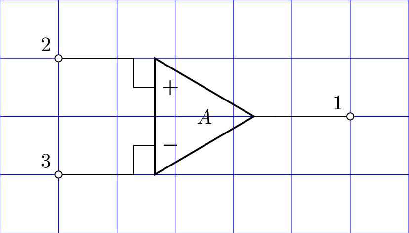
The size can be controlled with the scale and size options. The positions of the inverting and non-inverting inputs can be flipped with the mirror option.
E 1 0 opamp 2 3 A; right, scale=0.75, size=0.75
;help_lines=1
E 1 0 opamp 2 3 A; right, scale=0.75
;help_lines=1
E 1 0 opamp 2 3 A; right, scale=0.5
;help_lines=1
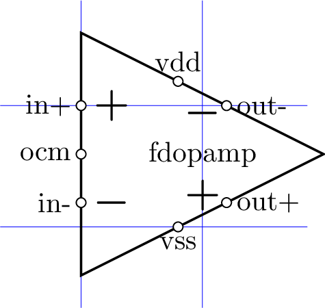
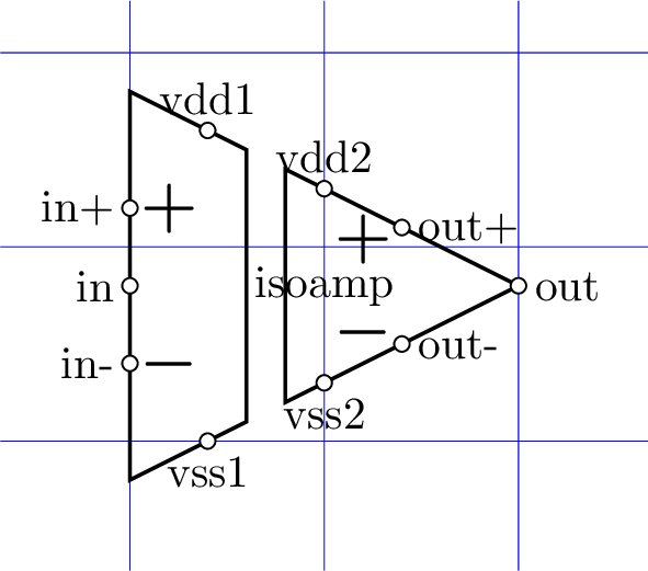
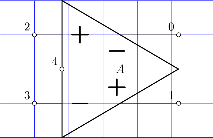
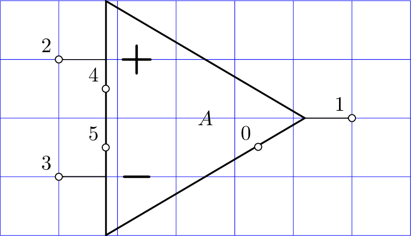
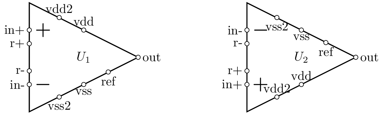
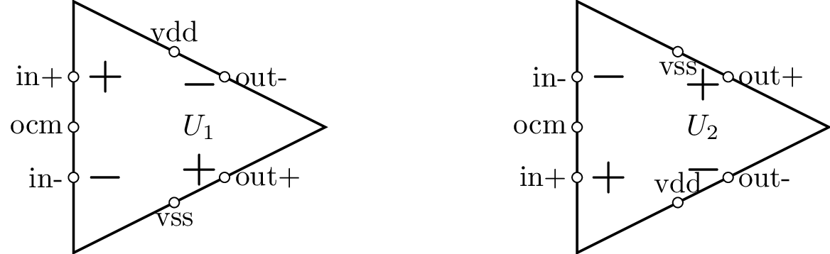
Fully differential opamps and instrumentation amplifiers can be drawn in a similar manner using the fdopamp or inamp argument to a VCCS. For example:
E1 1 0 fdopamp 2 3 4 A; right
;help_lines=1
E1 1 0 inamp 2 3 4 5 A; right
;help_lines=1
Opamps and fully differential opamps have additional pins that can be connected:
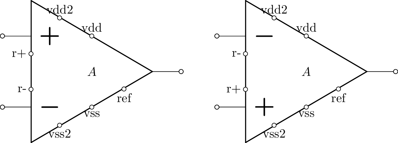
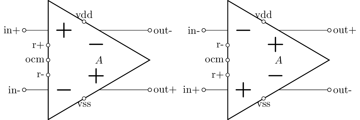
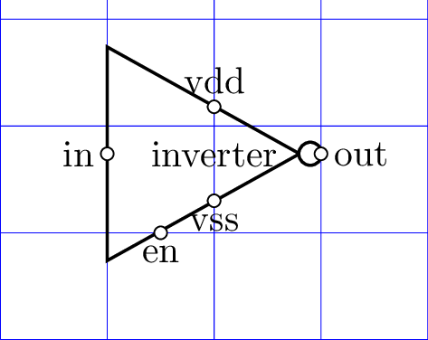
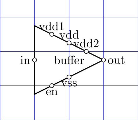
Opamps, fully differential opamps, and instrumentation amplifiers can also be drawn without the wires using the integrated circuit syntax. However, these cannot be analysed electrically. For example:
U1 opamp; right
U2 fdopamp; right
W U1.out U2.in+; right

Here are the named connections:
Potentiometers
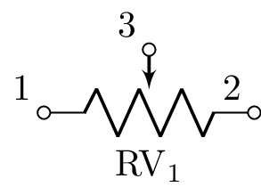
RV1 1 2 3; right
; label_nodes=all
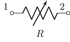
Alternatively, a variable resistor can be defined using:
R 1 2; variable
Reluctances
REL1 1 2; right
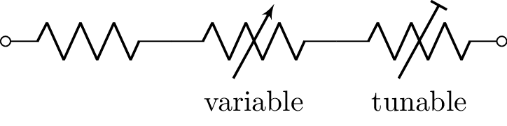
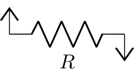
Resistors
R1 1 2; right, l=
R2 2 3; right, kind=variable, l=variable
R3 3 4; right, kind=tunable, l=tunable
; label_nodes=false, draw_nodes=connections
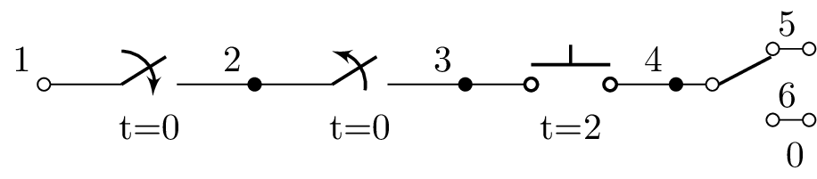
Switches
Switches can be drawn but they are ignored for analysis since they make the circuit time-varying.
The general format is:
SWname Np Nm nc|no|push
Here’s an example:
SW1 1 2 no; right
SW2 2 3 nc; right
SW3 3 4 push 2; right
SW4 4 5 6 spdt; right
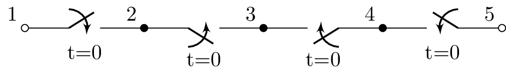
Switches can be mirrored and inverted, for example:
SW1 1 2 no; right
SW2 2 3 no; right, mirror
SW3 3 4 no; right, mirror, invert
SW4 4 5 no; right, invert
Transformers
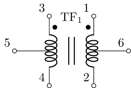
TF1 1 2 3 4; right
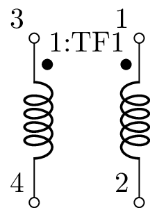
TF1 1 2 3 4 core; right
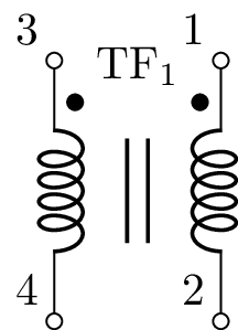
TF1 1 2 3 4 tap _5 _6; right
W 5 _5; right=0.5
W _6 6; right=0.5
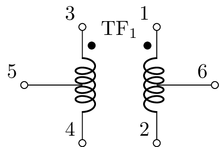
TF1 1 2 3 4 tapcore _5 _6; right
W 5 _5; right=0.5
W _6 6; right=0.5
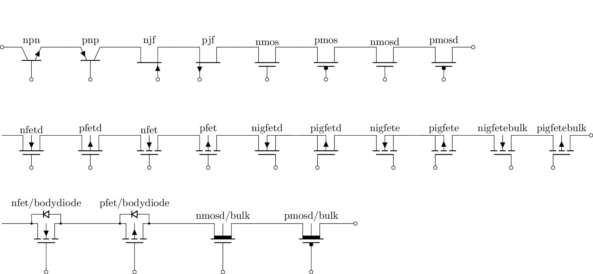
Transistors
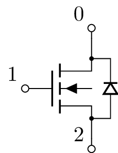
Transistors (BJT, JFET, and MOSFET) can be drawn but not analyzed. Both are added to the netlist using a syntax similar to that of SPICE. A BJT is described using:
Qname NC NB NE npn|pnp
where NC, NB, and NE denote the collector, base, and emitter nodes. A MOSFET is described using:
Mname ND NG NS nmos|pmos
where ND, NG, and NS denote the drain, gate, and source nodes.
A JFET is described using:
Jname ND NG NS njf|pjf
where ND, NG, and NS denote the drain, gate, and source nodes.
Here’s an example:
Q1 1 2 3 npn Q1; up, l=npn
Q2 4 5 3 pnp Q2; up, l=pnp
J1 4 6 7 njf J1; up, l=njf
J2 8 9 7 pjf J2; up, l=pjf
M1 8 10 11 nmos M1; up, l=nmos
M2 12 13 11 pmos M2; up, l=pmos
M3 12 14 15 nmos M3; up, l=nmosd
M4 16 17 15 pmos M4; up, l=pmosd

# Hack to include labels in bounding box
O 7 18; up=0.8

O 1 19; down=1.5

M5 19 20 21  M5; up, kind=nfetd, l=nfetd
M6 22 23 21  M6; up, kind=pfetd, l=pfetd
M7 22 24 25  M7; up, kind=nfet, l=nfet
M8 26 27 25  M8; up, kind=pfet, l=pfet
M9 26 28 29  M9; up, kind=nigfetd, l=nigfetd
M10 30 31 29  M10; up, kind=pigfetd, l=pigfetd
M11 30 32 33  M11; up, kind=nigfete, l=nigfete
M12 34 35 33  M12; up, kind=pigfete, l=pigfete
M13 34 36 37  M13; up, kind=nigfetebulk, l=nigfetebulk
M14 38 39 37  M14; up, kind=pigfetebulk, l=pigfetebulk

O 19 40; down=1.5

M15 40 41 42  M15; up=1.5, kind=nfet, l=nfet/bodydiode, bodydiode
M16 43 44 42  M16; up=1.5, kind=pfet, l=pfet/bodydiode, bodydiode
M17 43 45 46  M17; up=1.5, kind=nmosd, l=nmosd/bulk, bulk
M18 47 48 46  M18; up=1.5, kind=pmosd, l=pmosd/bulk, bulk
M19 47 49 50  M19; up=1.5, kind=nmos, l=nmos/arrowmos, arrowmos
M20 51 52 50  M20; up=1.5, kind=pmos, l=pmos/arrowmos, arrowmos

; label_nodes=none, draw_nodes=connections
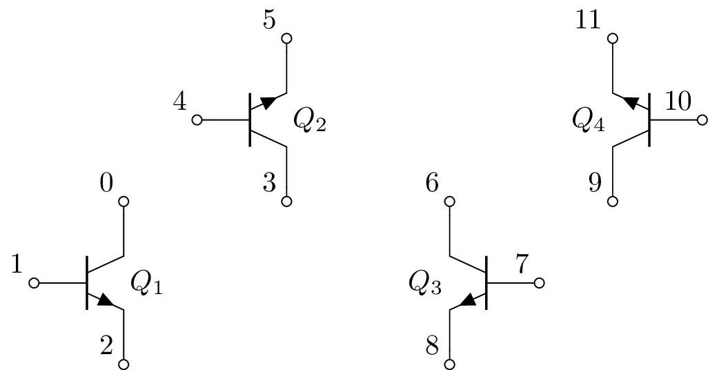
The transistors can be flipped up-down with the mirror attribute and left-right with the invert attribute, for example:
Q1 0 1 2; right
Q2 3 4 5; right, mirror
Q3 6 7 8; right, invert
Q4 9 10 11; right, mirror, invert

O 0 3; right
O 3 6; right
O 6 9; right
There are many variants of transistor that can be selected with the kind attribute. For example,
M1 0 1 2; right, kind=nfet, bodydiode
There are several kinds of bipolar transistor:
nigbt, pigbt n- and p-type L-shaped insulated gate bipolar transistor
Lnigbt, Lpigbt n- and p-type L-shaped insulated gate bipolar transistor
There are many kinds of MOSFET:
nmos, pmos simplified form of n- and p-channel enhancement mode MOSFETS
nmosd, pmosd simplified form of n- and p-channel depletion mode MOSFETS
nfet, pfet n- and p-channel enhancement mode MOSFETS
nfetd, pfetd n- and p-channel depletion mode MOSFETS
nigfete, pigfete n- and p-channel enhancement mode MOSFETS with insulated gate
nigfetd, pigfetd n- and p-channel depletion mode MOSFETS with insulated gate
nigfetbulk, pigfetbulk
hemt high-electron mobility transistor
Bipolar transistors have the following attributes:
bodydiode
schottky base
MOSFET transistors have the following attributes:
bodydiode
arrowmos
ferroel gate ferroelectric gate
See the Circuitikz manual for the various attributes that can be applied to transistors.
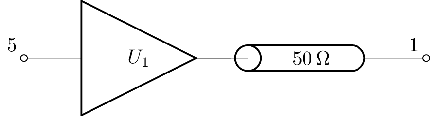
Transmission lines
A transmission line is a two-port device. Here’s an example:
U1 buffer; right
TL1 1 2 U1.out 4; right=2, scale=2, l={50\,$\Omega$}
R 1 2; down
W U1.vdd 9; up=0.1, implicit, l=Vdd
W U1.vss 11; down
W 11 4; right=0.5
W 11 10; down=0.1, implicit, l=Vss
W 5 U1.in; right=0.5
;draw_nodes=connections

The ground wires can be removed using the nowires attribute:
U1 buffer; right
TL1 1 2 U1.out 4; right=2, scale=2, l={50\,$\Omega$}, nowires
W 5 U1.in; right=0.5
;draw_nodes=connections
For more generic transmission lines see Cables.
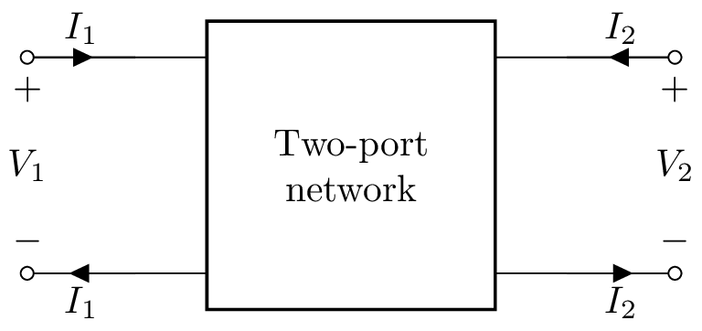
Two-port networks
A generic two-port network is described using:
TPname Np Nm Ncp Ncm
Ncp and Ncm define the positive and negative nodes of the control (input) port. Here’s an example:
TP1 1 2 3 4; right, l=Two-port network
W 1 1a; right=0.5, i^<=I_2
W 2 2a; right=0.5, i_=I_2
W 3a 3; right=0.5, i=I_1
W 4a 4; right=0.5, ir=I_1
P 1a 2a; down, v^=V_2
P 3a 4a; down, v_=V_1
; draw_nodes=none, label_nodes=none
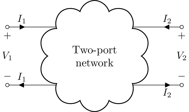
Here’s another example:
TP1 1 2 3 4; right, l=Two-port network, shape=cloud
W 1 1a; right=0.5, i^<=I_2
W 2 2a; right=0.5, i_=I_2
W 3a 3; right=0.5, i=I_1
W 4a 4; right=0.5, ir=I_1
P 1a 2a; down, v^=V_2
P 3a 4a; down, v_=V_1
; draw_nodes=none, label_nodes=none
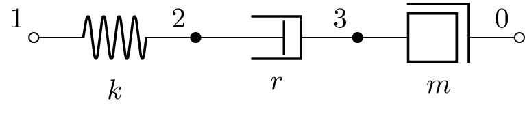
Mechanical components
Springs, dampers (dashpots), and masses are oneport components for modelling mechanical systems, for example,
k 1 2; right
r 2 3; right
m 3 0; right
Wires
Wires are useful for schematic formatting, for example,
W 1 2; right
Here an anonymous wire is created since it has no identifier.
The line style of wires can be changed, such as dashed or dotted (see Line styles).
Wires can be implicitly added using the offset attribute. Here’s an example to draw two parallel resistors:
R1 1 2; right, offset=0.25
R2 1 2; right, offset=-0.25
; draw_nodes=connections, label_nodes=none
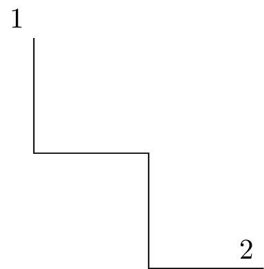
Stepped wires
Stepped wires can be drawn using the steps attribute. For example:
O 1 2; right=2, rotate=-45
W 1 2; steps=-|, free

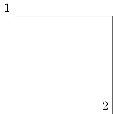
O 1 2; right=2, rotate=-45
W 1 2; steps=|-|-, free
In these examples, the free attribute is used so that the wire places no constraints on the node positions. Thus the size and rotate attributes are ignored. The open-circuit component is used to fix the node locations.
The - character represents a horizontal step and the | character represents a vertical step. The shape of the line is controlled by the step pattern. For example –|- represents two steps horizontally, one step vertically, and then one step horizontally. A number before the - or | symbol specifies the number of repeats of the step. For example, steps=-4|- is equivalent to steps=-||||-.
If the step pattern is not specified, a default step pattern -| is chosen if the horizontal extent is longer than the vertical extent and |- is chosen otherwise. For example,
O 1 2; right=2, rotate=-45
W 1 2; steps, free
Arrows
Arrows can be drawn on wires using the startarrow and endarrow attributes. There are many arrow styles, see the Tikz manual. For example,
W 1 2; right, endarrow=tri
W 2 3; right, endarrow=otri
W 3 4; right, startarrow=open triangle 90, endarrow=open triangle 90
W 4 5; right, startarrow=stealth, endarrow=stealth
; help_lines=1, draw_nodes=none
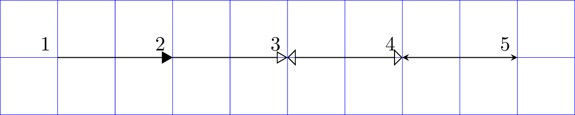
Autoground
If autoground set to True then implicit ground connections are automatically added for all the ground, 0, nodes. The type of ground connection can be specified, for example:
Iin 1 0 {6*u(t)+3*delta(t)}; down
W 1 2; size=1.5
R1 2 0 2; down
R2 2 3 1; size=1.5
L1 3 0 0.2; down
;label_ids=none, autoground=ground
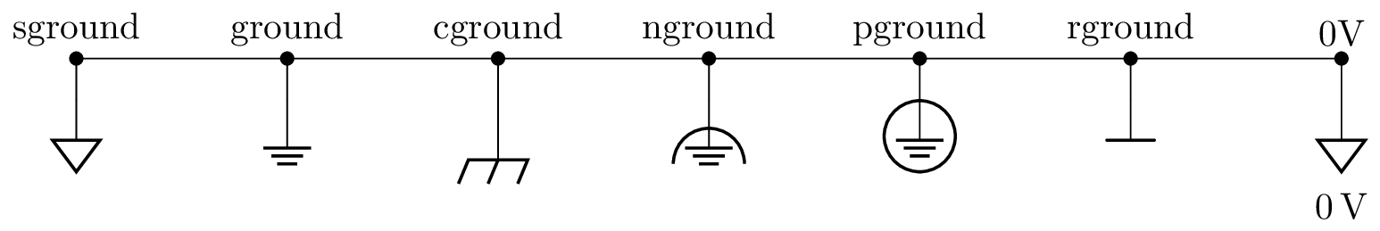
Implicit connections
Implicit connections are commonly employed for power supply and ground connections. They have one of the following attributes:
implicit equivalent to signal ground
sground signal ground
ground earth ground
cground chassis ground
nground noiseless ground
pground protected ground
rground reference ground
tlground tailless ground
tground thicker tailless ground
eground European style ground
eground2 alternative European style ground
0V ground
vcc positive power supply (voltage to collectors)
vdd positive power supply (voltage to drains ;-)
vee negative power supply (voltage to emitters)
vss negative power supply (voltage to sources)
Implicit connections can be added to any oneport netlist component (resistor, capacitor, wire, etc.), for example:
R1 1 2; down, vdd, l={24\,V}
R2 2 3; down, vss
R3 2 4; right, sground
The first node is considered the implicit wire for vcc and vdd otherwise it is the last node. The node can also be specified, for example:
M1 1 2 3; right, kind=nfet, .s.vss, .s.l={0\,V}
R 4 1; down, .p.vdd, .p.l={10\,V}
W 1 5; right=0.5

In this example, the MOSFET has three nodes: d (drain), g (gate), and s (source). The resistor has two nodes: p (positive) and n (negative).
Here are some ground examples:
# signal ground
W 1 01; down=0.2, sground
A 1; l=sground, anchor=s
W 1 2; right
# earth ground
W 2 02; down=0.2, ground
A 2; l=ground, anchor=s
W 2 3; right
# chassis ground
W 3 03; down=0.2, cground
A 3; l=cground, anchor=s
W 3 4; right
# noiseless ground
W 4 04; down=0.2, nground
A 4; l=nground, anchor=s
W 4 5; right
# protected ground
W 5 05; down=0.2, pground
A 5; l=pground, anchor=s
W 5 6; right
# reference ground
W 6 06; down=0.2, rground
A 6; l=rground, anchor=s
W 6 7; right
# 0V
W 7 07; down=0.2, 0V
A 7; l=0V, anchor=s
; label_nodes=none
; draw_nodes=none
# tailless ground
W 1 01; down=0.2, tlground
A 1; l=tlground, anchor=s
W 1 2; right
# thick tailless ground
W 2 02; down=0.2, tground
A 2; l=tground, anchor=s
W 2 3; right
# European ground
W 3 03; down=0.2, eground
A 3; l=eground, anchor=s
W 3 4; right
# alternative European ground
W 4 04; down=0.2, eground2
A 4; l=eground2, anchor=s
; label_nodes=none
; draw_nodes=none

Here are some power supply examples:
R 1 2; right, .p.vcc, .n.vee
Signal connections
These are similar to implicit power connections but are useful for denoting an off-sheet connection or an IC pin. They have one of the attributes:
input input connection
output output connection
bidir bidirectional connection
pad generic connection
For example:
W 1 2; right=0.2, input, l=input, fill=blue!50
W 3 4; right=0.2, output, l=output
W 5 6; right=0.2, bidir, l=bidir
W 7 8; right=0.2, pad, l=pad
O 1 3; right
O 3 5; right
O 5 7; right
; draw_nodes=connections, label_nodes=none

The sizes of the pads can be controlled with the width and aspect attributes.
For example:
W 1 2; right=0.2, output, l=PA0, fill=blue!50
W 3 4; right=0.2, output=1.25, l=PA0
W 5 6; right=0.2, output=1.25, l=PA0, aspect=1.25
W 7 8; right=0.2, output, l=PA0, aspect=0.8
O 1 3; right=1.5
O 3 5; right=1.5
O 5 7; right=1.5

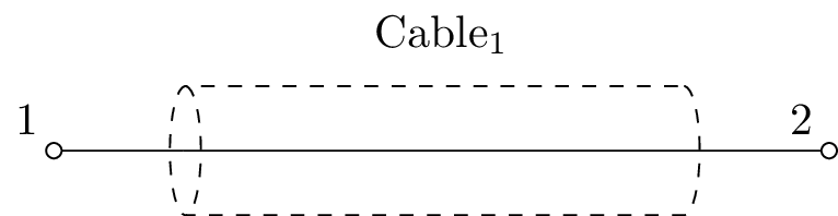
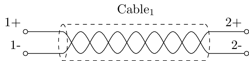
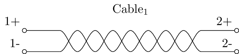
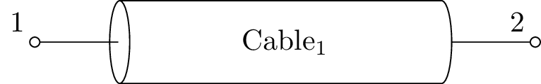
Cables
The kind of cable is specified with the kind attribute. This can be coax, twinax, twistedpair, shieldedtwistedpair, or tline (transmission line). The default is coax. Note, this component is experimental and the syntax may change.
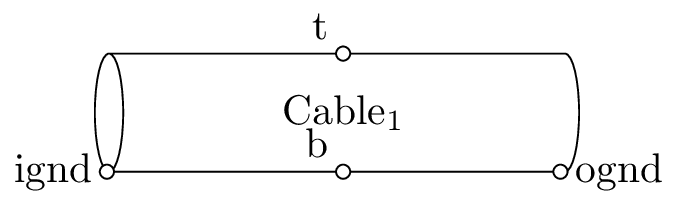
Here are some examples:
Cable1; right=2, dashed, kind=coax
W 1 Cable1.in; right=0.5
W Cable1.out 2; right=0.5
Cable1; right=2, dashed, kind=twinax
W 1+ Cable1.in+; right=0.5
W 1- Cable1.in-; right=0.5
W Cable1.out+ 2+; right=0.5
W Cable1.out- 2-; right=0.5
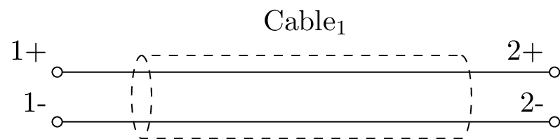
Cable1; right=2, dashed, kind=shieldedtwistedpair
W 1+ Cable1.in+; right=0.5
W 1- Cable1.in-; right=0.5
W Cable1.out+ 2+; right=0.5
W Cable1.out- 2-; right=0.5
Cable1; right=2, dashed, kind=twistedpair
W 1+ Cable1.in+; right=0.5
W 1- Cable1.in-; right=0.5
W Cable1.out+ 2+; right=0.5
W Cable1.out- 2-; right=0.5
Cable1; right=2, kind=tline
W 1 Cable1.in; right=0.5
W Cable1.out 2; right=0.5
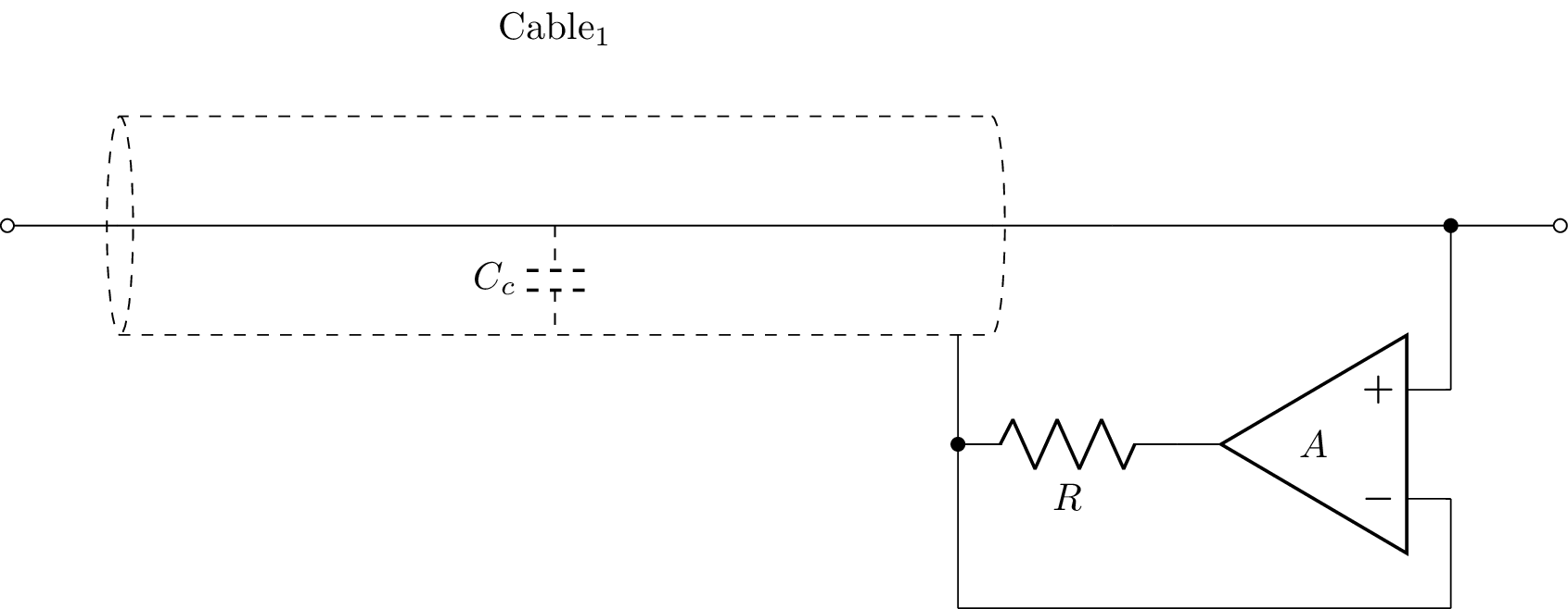
Cable1; right=4, dashed, kind=coax
W 1 Cable1.in; right=0.5
W Cable1.out 2; right=0.5
# Provide electrical connection
W Cable1.in Cable1.out; free, invisible
W Cable1.ognd 10; down=0.5
Cc Cable1.mid Cable1.b; down=0.2, dashed, scale=0.6
W 2 3; right=1.5
W 3 11; right=0.5
W 3 4; down=0.5
W 5 6; down=0.5
W 6 7; left
W 7 10; up=0.5
R 10 8; right
E 8 0 opamp 4 5 A; left=0.5, mirror, scale=0.5
; label_nodes=none, draw_nodes=connections
Block diagrams
- Block diagrams can be constructed with the following components:
BL – block (see Blocks)
TF – transfer function
SPpp, SPpm, SPppp, SPpmm, SPppm – summing points
MX – mixer
box – rectangular box
circle – circle (or ellipse)
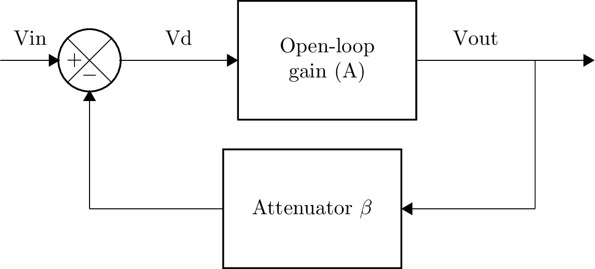
Here’s an example showing negative feedback:
W 1 14; right=0.5, endarrow=tri, l=V{in}
SP1 pm 14 9 13; right, l={}
W 13 10; endarrow=tri, l=Vd
TR1 10 11 A; right=1.5, l=Open-loop gain (A)
W 11 2; right, l=V{out}
W 2 3; down
TR2 8 12 B; left=1.5, l=Attenuator $\beta$
W 3 8; left, endarrow=tri
W 12 4; left
W 4 9; up, endarrow=tri
W 2 5; right=0.5, endarrow=tri
; draw_nodes=false, label_nodes=false
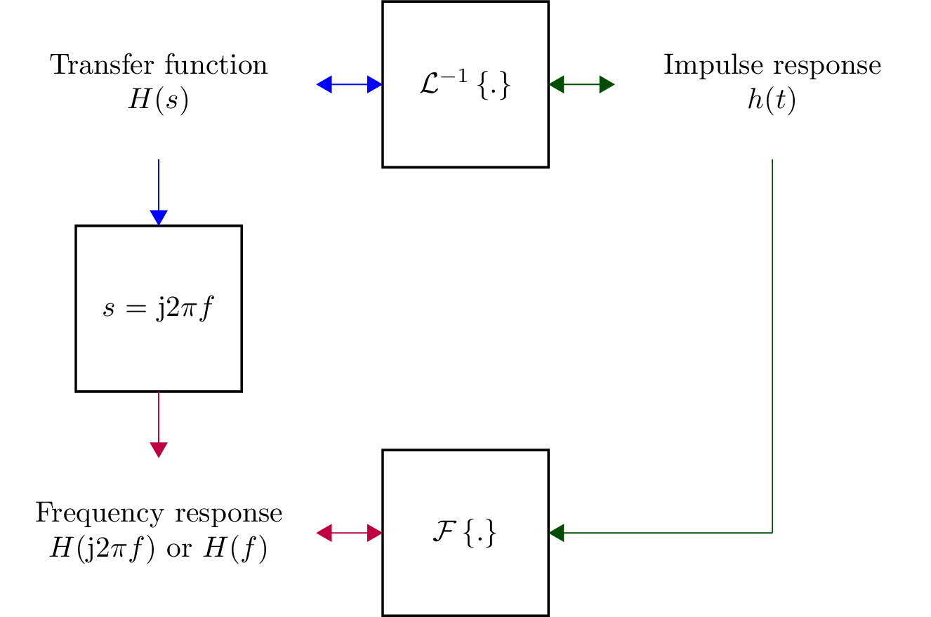
Here’s a more complicated example for a causal system:
S1 box; right=1.9, aspect=2.1, draw=white, l={Transfer function\\$H(s)$}
S2 box; right=1.9, aspect=2.1, draw=white, l={Impulse response\\$h(t)$}
S3 box; right=1.9, aspect=2.1, draw=white, l={Frequency response\\$H(\mathrm{j}2\pi f)$ or $H(f)$}
S4 box; right, l={$\mathcal{L}^{-1}\left\{.\right\}$}
S5 box; right, l={$\mathcal{F}\left\{.\right\}$}
S6 box; right, l={$s=\mathrm{j}2\pi f$}
W S1.e S4.w; right=0.4, startarrow=tri, endarrow=tri, color=blue
W S4.e S2.w; right=0.4, startarrow=tri, endarrow=tri, color=black!70!green
W S2.s 4; down, color=black!70!green
W 4 S5.e; left=0.4, endarrow=tri, color=black!70!green
W S5.w S3.e; left=0.4, startarrow=tri, endarrow=tri, color=purple
W S1.s S6.n; down=0.4, endarrow=tri, color=blue
W S6.s S3.n; down=0.4, endarrow=tri, color=purple
O S4.mid S5.mid; down=1.3
; label_nodes=alpha, draw_nodes=none, label_ids=false
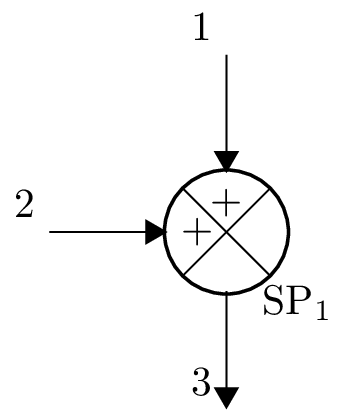
Summing points
There are a number of summing point varieties: SPpp, SPpm, SPppp, SPpmm, SPppm. The p suffix stands for plus, the m suffix stands for minus. The other variations can be generated using the mirror attribute.
Here’s an example:
SP1 pp ._1 ._2 ._3; down
W 1 SP1._1; down=0.5, endarrow=tri
W 2 SP1._2; right=0.5, endarrow=tri
W SP1._3 3; down=0.5, endarrow=tri
; draw_nodes=false
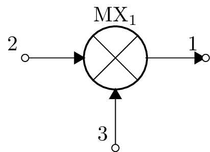
Mixers
Here’s a example of a mixer:
MX1 ._1 ._2 ._3; right
W MX1._1 1; right=0.5, endarrow=tri
W 2 MX1._2; right=0.5, endarrow=tri
W 3 MX1._3; up=0.5, endarrow=tri
Shapes
Shapes include box, circle, ellipse, and triangle.
box, circle, ellipse, and triangle shapes have connection pins based on the centre (c) and sixteen directions of the compass: n, nne, ne, ene, e, ese, se, sse, s, ssw, sw, wsw, w, wnw, nw, nww. For other rectangular shapes see Integrated circuits.
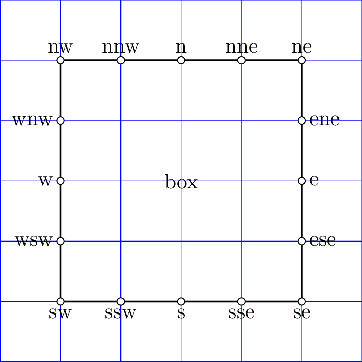
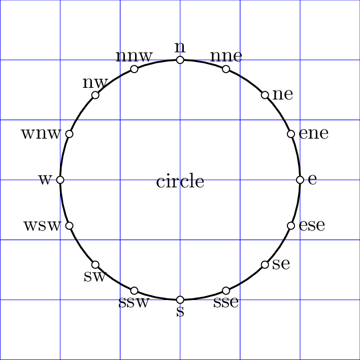
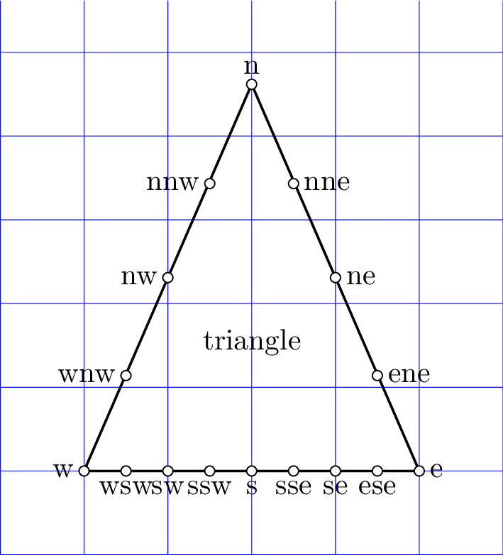
The aspect ratio of box, circle, and triangle can be controlled with the aspect attribute.
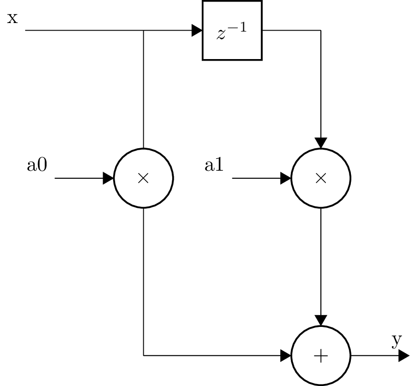
Here’s an example of their use:
W x 1; right
W 1 S1.w; right=0.5, endarrow=tri
S1 box; right=0.5, l=$z^{-1}$
S2 circle; right=0.5, l=$\times$
S3 circle; right=0.5, l=$\times$
S4 circle; right=0.5, l=$+$
W S1.e 2; right=0.5
W 3 S4.w; right=1.25, endarrow=tri
W 1 S2.n; down
W S2.s 3; down
W a0 S2.w; right=0.5, endarrow=tri
W 2 S3.n; down, endarrow=tri
W S3.s S4.n; down, endarrow=tri
W a1 S3.w; right=0.5, endarrow=tri
W S4.e y; right=0.5, endarrow=tri
# Align multipliers
O S2.w S3.w; right
; draw_nodes=false, label_nodes=alpha
triangle is an equilateral triangle. Its shape can be changed with the aspect attribute. It has connection pins n, e, s, w, c, c1, c2, c3.
The label of a shape can be replaced by an image, using the image attribute. For example,
S1 box; right=4, image=cmos1.png
The image file can be of any format supported by the LaTeX \includegraphics macro (such as .pdf, .png, .jpg, etc) or a file that can be processed by LaTeX with the \input macro (such as .pgf, .tex, .schtex).
Each shape or chip have the following connection pins:
tl (top left)
tr (top right)
bl (bottom left)
br (bottom right)
mid (middle)
In addition, there are component specific connection pins. Associated with each pin is an optional label.
- The pinlabels option can be specified as:
all : the labels for all the pins are shown
connected : the labels for all the connected pins are shown
default : the default labels are shown (default)
none : none of the labels are shown
{pin1:label1, pin2:label2, …}: the labels are specified for the named pins.
- The names of the pins can be drawn using the pinnames option. This has a syntax:
all : the pin names for all the pins are shown
connected : the pin names for all the connected pins are shown
none : none of the pin names are shown (default)
{pin1, pin2, …} : the specified pin names are shown.
- The nodes of the pins can be drawn using the pinnodes option. This has a syntax:
all : the pin nodes for all the pins are shown
connected : the pin nodes for all the connected pins are shown
none : none of the pin nodes are shown (default)
{pin1, pin2, …} : the specified pin nodes are shown.
- The pin names can be redefined by the pindefs option. This has a syntax:
pindefs={new1=old1, new2=old2, …}
Styles
Three component styles are supported: american (default), british, and european. The style is set by a style argument to the draw method. For example:
>>> cct.draw(style='european')
Alternatively the style can specified by a schematic option. For example:
Vi 1 0_1; down
Rs 1 2; right=1.5
C 2 0; down
W 0_1 0; right
W 0 0_2; right
Rin 2_2 0_2; down, v=V_{in}
W 2 2_2; right
E1 3 0_3 2 0 A; down, l=A V_{in}
Rout 3 4; right=1.5
RL 4 0_4; down, v=V_o
W 0_2 0_3; size=1.3
W 0_3 0_4
P1 4 0_4; down
; style=european

The style of inductors, resistors, current sources, and voltage sources can be overridden with inductor_style, resistor_style, current_source_style, and voltage_source_style. These can be american or european. In addition, the inductor style can be cute.
Here’s an example (I wonder who would do this?):
R 1 2; right
L 2 3; right
I1 3 4; right
V 4 5; right
; label_nodes=false, draw_nodes=connections, resistor_style=european
; inductor_style=american, voltage_source_style=american, current_source_style=european

Colors
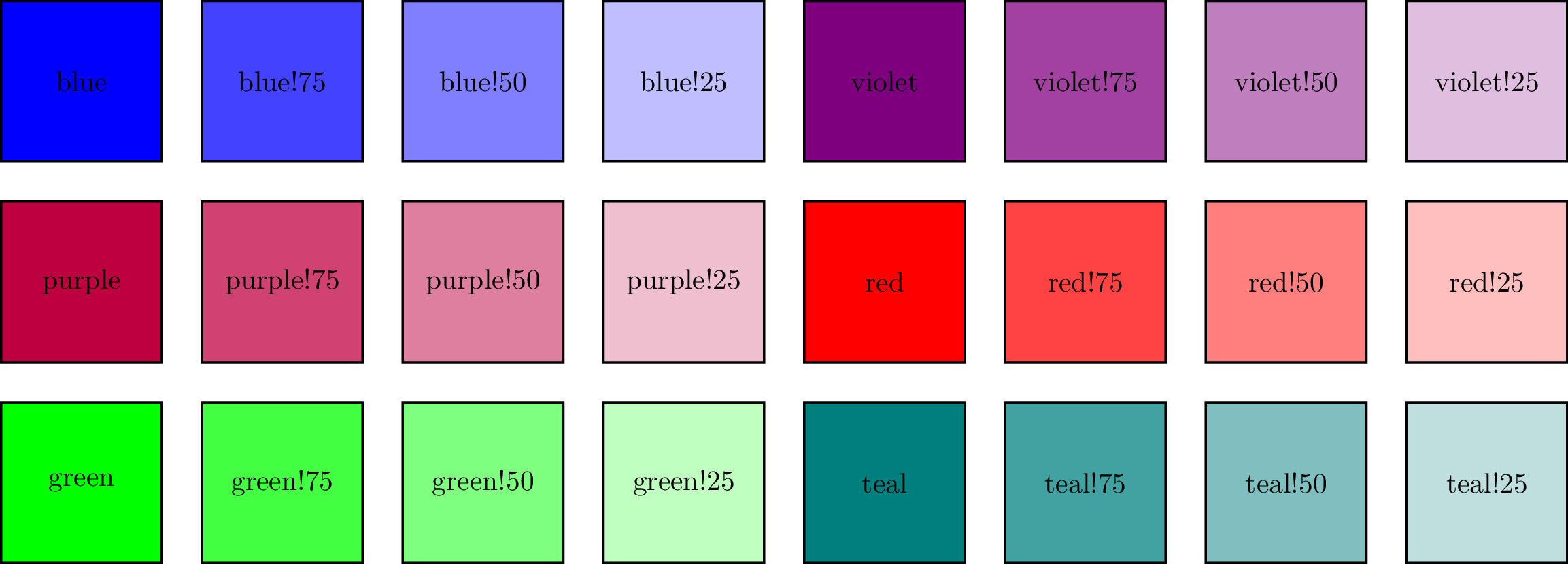
By default the components are drawn in black. This can be overridden with the color attribute, for example:
>>> cct.add('R1 1 2; right, color=blue')
Colors can be specified many ways, see https://en.wikibooks.org/wiki/LaTeX/Colors and https://latexcolor.com/.
Here are some examples using the fill attribute:
Shading can be performed using the top color and bottom color attributes, see the Tikz manual.
Line styles
The line style of wires can be changed using the Tikz attributes, dashed, dotted, thick, ultra thick, line width, densely dotted, loosely dashed and many others. For example,
W 1 2; right
W 2 3; right, dashed
W 3 4; right, dotted
W 4 5; right, thick
W 5 6; right, ultra thick
W 6 7; right, ultra thick, dashed
W 7 8; right, line width=4pt
; help_lines=1
Attribute definitions
New attributes can be created with the def attribute. For example:
; def highlight={color=blue, thick}
This defines a new attribute called highlight. Any following occurrences of this in the netlist is replaced by color=blue, thick. For example:
R1 1 2; right, highlight
is equivalent to:
R1 1 2; right, color=blue, thick
Labels and annotations
Both components and nodes can be labelled and and annotated. In addition, arbitrary Circuitikz/Tikz macros can be applied to embellish a schematic.
Component labels and annotations
Each component has a component identifier label and a value label. These can be augmented by explicit voltage, current, and flow labels. One-port components (bipoles) also have an optional annotation that is similar to a label. Some components have an inner label.
l=label – component label
l2=label1 and label2 – vertically stack labels label1 and label2
a=label – annotation
a2=label1 and label2 – vertically stack annotations label1 and label2
t=label – inner label
i=label – current label
v=label – voltage label
f=label – flow label
The label can be displayed using LaTeX math-mode by enclosing the label between dollar signs. Thus superscripts and subscripts can be employed. For example,
>>> cct.add('R1 1 2; right, i=$I_1$, v=$V_{R_1}$')
Math-mode labels need to be enclosed in $…$. Words in sub- and superscripts are converted into a roman font using mathrm. This feature is also activated if the label is not enclosed in $…$ but includes an ^ or _.
Lcapy will try to automatically switch to math-mode if it detects a math-mode command. Use \mathrm{} to ensure text is kept in a Roman text font rather than an italic math font.
The component label and annotation positions are controlled with the ^ and _ attributes. The ^ attribute positions the label above the component and the _ attribute positions the label below the component. For example,
R1 1 2; right=1.5, l=A
R2 2 3; right=1.5, l_=B
R3 3 4; right=1.5, l^=C
; label_nodes=none, draw_nodes=none
Component annotations are similar to a component label but use the a attribute instead of the l attribute, for example,
R1 1 2;
R2 2 3; a={1\,k}
R3 3 4; a_={1\,k}, l^=R_2
; label_nodes=none, draw_nodes=none, node_spacing=3
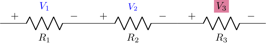
The style of the labels can be changed with the bipole label style attribute. Similarly, the style of the annotation, voltage, current, and flow labels can be changed with the bipole annotation style, bipole voltage style, bipole current style, and bipole flow style attributes. For example,
R1 1 2; right=1.5, v=V_1, bipole voltage style={color=blue}
R2 2 3; right=1.5, v=V_2, bipole voltage style={color=blue, font=\small}
R3 3 4; right=1.5, v=V_3, bipole voltage style={fill=purple!50}
; label_nodes=none, draw_nodes=none
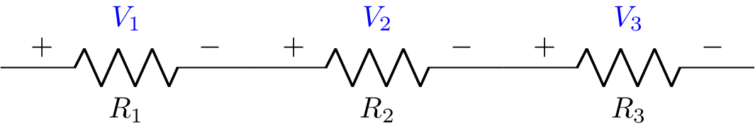
These styles can be applied to the entire schematic, for example,
R1 1 2; right=1.5, v=V_1
R2 2 3; right=1.5, v=V_2
R3 3 4; right=1.5, v=V_3
; label_nodes=none, draw_nodes=none, bipole voltage style={color=blue}
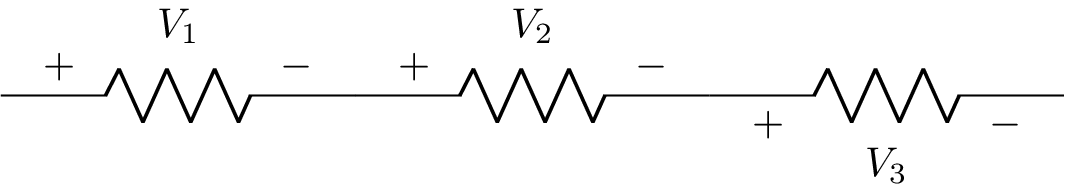
Voltage labels
Voltage label positions are controlled with the ^ and _ modifiers. The ^ modifier positions the label above the component and the _ modifier positions the label below the component. For example,
R1 1 2; right=1.5, v=V_1, l=
R2 2 3; right=1.5, v^=V_2, l=
R3 3 4; right=1.5, v_=V_3, l=
; label_nodes=none, draw_nodes=none
An exception is for open-circuit or port components where the voltage label is drawn directly between the nodes.
The direction of the voltage labels depends on the voltage dir attribute. This can be RP for rising potential or EF for electric field. RP is the default.
Voltage labels can be annotated between pairs of nodes using an open-circuit component. For example,
>>> O1 1 0; down, v=V_1
Current and flow labels
The current and flow labels have additional < and > modifiers to specify the flow direction. If these come before the ^ and _ modifiers, the label is positioned at the start of the component otherwise it is positioned at the end of the component.
Here are some examples of current and flow label positioning:
R1 1 2; right=1.5, i=I, l=
R2 2 3; right=1.5, i>^=I, l=$>\wedge$
R3 3 4; right=1.5, i>_=I, l=$>\_$
R4 4 5; right=1.5, i^>=I, l=$\wedge>$
R5 5 6; right=1.5, i_>=I, l=$\_>$
R6 6 7; right=1.5, i<^=-I, l=$<\wedge$
R7 7 8; right=1.5, i<_=-I, l=$<\_$
R8 8 9; right=1.5, i^<=-I, l=$\wedge<$
R9 9 10; right=1.5, i_<=-I, l=$\_<$
; label_nodes=none, draw_nodes=none

R1 2 1; left=1.5, i=I, l=
R2 3 2; left=1.5, i>^=I, l=$>\wedge$
R3 4 3; left=1.5, i>_=I, l=$>\_$
R4 5 4; left=1.5, i^>=I, l=$\wedge>$
R5 6 5; left=1.5, i_>=I, l=$\_>$
R6 7 6; left=1.5, i<^=-I, l=$<\wedge$
R7 8 7; left=1.5, i<_=-I, l=$<\_$
R8 9 8; left=1.5, i^<=-I, l=$\wedge<$
R9 10 9; left=1.5, i_<=-I, l=$\_<$
; label_nodes=none, draw_nodes=none

R1 1 2; right=1.5, f=I, l=
R2 2 3; right=1.5, f>^=I, l=$>\wedge$
R3 3 4; right=1.5, f>_=I, l=$>\_$
R4 4 5; right=1.5, f^>=I, l=$\wedge>$
R5 5 6; right=1.5, f_>=I, l=$\_>$
R6 6 7; right=1.5, f<^=-I, l=$<\wedge$
R7 7 8; right=1.5, f<_=-I, l=$<\_$
R8 8 9; right=1.5, f^<=-I, l=$\wedge<$
R9 9 10; right=1.5, f_<=-I, l=$\_<$
; label_nodes=none, draw_nodes=none

By default, if a component has a value label it is displayed, otherwise the component identifier is displayed. Both can be displayed using:
>>> cct.draw(label_ids=True, label_values=True)
Schematic options are separated using a comma. If you need a comma, say in a label, enclose the field in braces. For example:
>>> C1 1 0 100e-12; down, size=1.5, v={5\,kV}
Label formatting
Component labels are comprised of a component name and a component value. If the names are the same, the component value is not shown. Display of the component name is controlled by the label_ids attribute and display of the component value is controlled by the label_values attribute.
There are several label formatting styles controlled by the label_style attribute:
‘aligned’: The component name and component value are separated by ‘=’:
R1 1 2 10; right
; label_style=aligned

‘stacked’: The component name is displayed above the component value:
R1 1 2 10; right
; label_style=stacked

‘split’: The component name and value are displayed on either side of the component using the ‘split’ style:
R1 1 2 10; right
; label_style=split
‘name’: Only the component name is displayed:
R1 1 2 10; right
; label_style=name

‘value’: Only the component value is displayed.
R1 1 2 10; right
; label_style=value

The component name and value can be overridden with the ‘l’ attribute.
Label value style
Label values are formatted according to the label_value_style attribute. The default is eng3 which uses an engineering format with a maximum of three digits. Other formats include spice, sci (scientific), and ratfun (rational functions), and sympy, see Number formatting.
Here’s an example showing the different formats:

Label placement
The component label placement depends on the direction the component is drawn. For a component drawn to the right, the label is placed below the component and the voltage label is placed above the component, for example:
R1 1 2; right, v=V_1
R2 2 3; down, v=V_2
R3 3 4; left, v=V_3
R4 4 1; up, v=V_4
; label_nodes=none, draw_nodes=none, node_spacing=3

This labels position be swapped using the label_flip attribute, for example:
R1 1 2; right, v=V_1
R2 2 3; down, v=V_2
R3 3 4; left, v=V_3
R4 4 1; up, v=V_4
; label_nodes=none, draw_nodes=none, node_spacing=3, label_flip=true

The annotation label is placed on the other side of the component to the component label. However, this can conflict with the voltage label.
Node annotations
Nodes can be annotated using the A net. For example,
R 1 2; right
A1 1; l=hello, anchor=north
A2 2; l=world, anchor=west
; label_nodes=false

The annotation is positioned with respect to the node using the anchor attribute. This can be north, north east, east, south east, south, south west, west, and north west or the abbreviations n, ne, e, se, s, sw, w and nw. The annotation point can be shifted with the xoffset and yoffset attributes and rotated with the rotate attribute. For example,
S1 box; l=Box
A S1.mid; yoffset=0.5, l=Top label, anchor=s
A S1.mid; yoffset=-0.5, l=Bottom label, anchor=n
; label_nodes=false

Another way to label a node is using a node label attribute (see Node attributes). For example, R 1 2; right .+.l=foo. This labels the positive node with foo. The position can be adjusted using an anchor: R 1 2; right .+.l=foo .+.anchor=south.
Miscellaneous annotation
Schematics can be also annotated using additional Tikz commands in the netlist. These are delimited by a line starting with two semicolons. A common use is for box fitting.
Box fitting
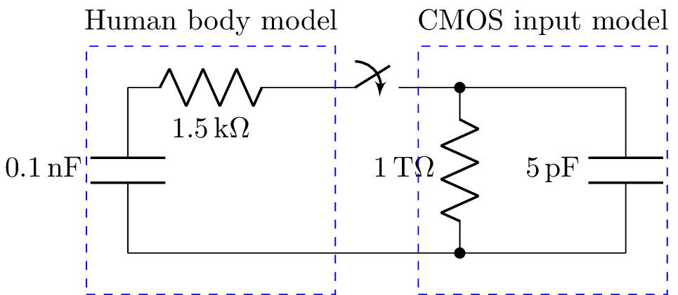
Boxes can be drawn around components and groups of components using Tikz macros defined in the netlist. For example:
C1 1 0 100e-12;down
R1 1 6 1500;right
R2 2 4 1e12;down
C2 3 5 5e-12;down
W 2 3;right
W 0 4;right
W 4 5;right
SW 6 2 no;right, l=
;;\node[blue,draw,dashed,inner sep=5mm,anchor=north, fit=(1) (6) (0), label=Human body model] {};
;;\node[blue,draw,dashed,inner sep=5mm, fit=(2) (3) (4) (5), label=CMOS input model]{};
;draw_nodes=connections, label_nodes=False, label_ids=False
This example draws dashed boxes around the nodes 0, 1, and 6 and 2, 3, 4, and 5:
Alternatively, the boxes can be fit around named components, for example:
;;\node[blue,draw,dashed,inner sep=5mm, fit=(R2) (C2), label=CMOS input model]{};
With this example, the netlist must be stored in a file or as a raw string to avoid the \n being interpreted as a new line. For example,
>>> a = Circuit(r"""
;;\node[blue,draw,dashed,inner sep=5mm, fit=(R2) (C2), label=CMOS input model]{};
""")
Boxes can be fitted around pin connections of components. When referring to a pin connection of a component it is necessary to use @ instead of ., for example, U1@tl instead of U1.tl. Here’s an example:
U1 chip3333; right, l={MCU}, pinlabels={vss,vdd}
R1 1 1a; down
V_DD 1a 0; down
L1 1 2; right=1
L2 0 0_2; right
W 2 5; right=0.5
W 0_2 0_5; right=0.5
Cbulk 5 0_5; down=2, kind=electrolytic
L3 5 6; right
L4 0_5 0_6; right
W 6 3; right=0.5
W 0_6 0_3; right=0.5
L5 3 4; right, color=blue
L6 0_3 0_4; right, color=blue
W 4 U1.vdd; down=0.25, color=blue
W 0_4 U1.vss; up=0.25, color=blue
Clocal 6 0_6; down, color=blue
A U1.tl
A U1.br
;;\node[blue,draw,dashed,inner sep=8mm, fit=(Cbulk) (U1@tl) (U1@br), label=PCB]{};
; label_nodes=none, draw_nodes=connections, label_values=false, label_ids=false
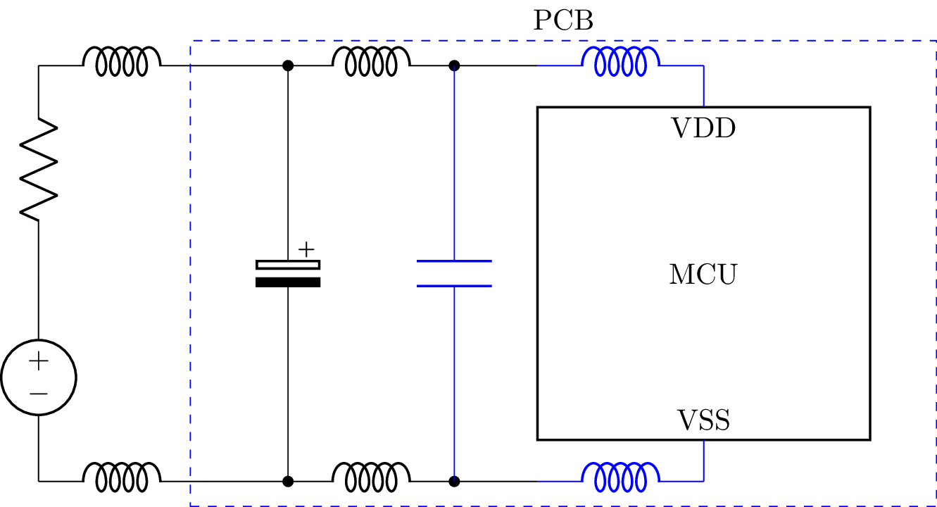
In this example, the node annotation entries (see Node annotations) make references to the top left (tl) and bottom right (br) coordinates of the U1 component. These references are required for the fit command.
Attributes
There are component attributes, node attributes, and schematic attributes. The precedence (highest to lowest) is:
node attributes
attributes specified as keyword arguments to the draw() method that are not None
component attributes
schematic attributes
default attributes
Component attributes
a: annotation (a second label) (also a^ and a_)
anchors: specify which anchors to show
aspect: aspect ratio for boxes
color: component color
f: flow label (also f, f_, f^, f_>, f_<, f^>, f^<, f>_, f<_, f>^, f<^, f>, f<)
fill: component fill color
fliplr: flip left/right (horizontally)
flipud: flip up/down (vertically)
free: place no constraints on the node positions; this is useful for stepped wires. With this attribute the size and rotate attributes are ignored.
i: current label (also i, i_, i^, i_>, i_<, i^>, i^<, i>_, i<_, i>^, i<^, i>, i<, ir)
ignore: do not connect to the other components and do not draw (this is useful for simulating multiple mutual inductances but where it is too hard to show them on a schematic, see also nodraw and invisible)
invert: invert component vertically
invisible: connect to the other components but do not draw (see also nodraw and ignore)
fixed: do not stretch
kind: electrolytic, polar, or variable for capacitors; variable, choke, twolineschoke for inductors
l: label
mirror: mirror component in x-axis (opamps, transistors)
mirrorinputs: mirror inputs for opamps
nodraw: connect to the other components, generate the CircuiTikz macros, but do not include the draw argument (see also invisible and ignore)
nosim: this is ignored for schematics (it is used to ignore electrical simulation of the component)
offset: distance to orthogonally offset component (useful for parallel components)
pins: define pin labels for ICs
rotate: angle in degrees to rotate component anti-clockwise
size: scale factor for distance between component’s nodes
scale: scale factor for length of component
t: inner label
v: voltage label (also v, v_, v^, v_>, v_<, v^>, v^<, v<, v>)
variable: for variable resistors, inductors, and capacitors
width: specify component width
Here’s an example using the variable attribute:
V 1 0 ac; down=1.5
L 1 2; right=1.5, variable
R 2 3; down, variable
W 0 3; right
W 2 2_1; right
W 3 3_1; right
C 2_1 3_1; down, variable
See also the Circuitikz manual for other component attributes.
Node attributes
Node attributes are prefixed by a dot followed by the node name. For example, .p.vdd, .s.vss, .drain.output.
Oneport components such as resistors, voltage sources, capacitors, inductors, wires, etc., have two nodes: the first node (the positive node) is called p or + and the second node (the negative node) is called n or -. BJTs have c or collector, b or base, and e or emitter nodes. JFETs and MOSFETs have d or drain, g or gate, and s or source nodes. For chip node names, see Integrated circuits.
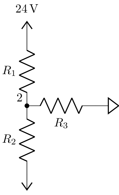
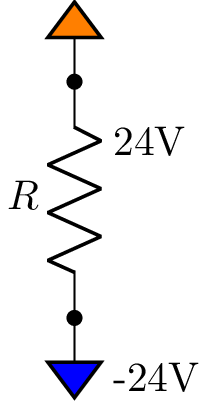
Here’s an example where the positive (+) node of a resistor is an implicit connection to +24 V and the negative (-) node of the resistor is an implicit connection to -24 V.
R 1 2; down, .-.implicit, .-.l=-24V, .-.fill=blue, .+.implicit, .+.l=24V, .+.fill=orange
Here’s another example using Signal connections:
U1 buffer; right, l=
W 1 U1.in; right=0.5, .+.input, .+.l=in, .+.fill=red!50
W U1.out 2; right=0.5, .-.output, .-.l=out, .-.fill=blue!50
; draw_nodes=connections, label_nodes=none
Schematic attributes
Schematic attributes apply to the whole schematic. They can be specified by starting a netlist entry with a semicolon, for example,
; help_lines=1, draw_nodes=connections, color=blue
For historical reasons, schematic attributes specified in the last entry of the netlist are considered first. These attributes override default attributes. Schematic attributes can be defined anywhere in the netlist and apply to the following netlist entries. They can be overridden by component attributes.
For example, consider the following netlist:
R1 1 2; right
; color=green
R2 2 3; right
R3 3 4; right
; color=red
R4 4 5; right
R5 5 6; right, color=purple
R6 6 7; right
; color=blue
This draws R1 in blue, R2 and R3 in green, R4 and R6 pin red, and R5 in purple. In this example, R5 has a component color attribute.
Note, nodes are drawn and labelled using the attributes current at their first definition.
The schematic attributes can be overridden using arguments to the draw method. For example,
>>> sch.draw(color='black')
Here is a list of the schematic attributes:
autoground: enables automatically drawing of implicit ground connections. Its argument can specify the type of connection (ground, sground, rground, etc). If the argument is False this feature is disable. If the argument is True, this feature is enabled using the the default symbol sground.
color: component colour (default black)
cpt_size: length of component (default 1.5).
dpi: dots per inch (default 150) when converting to a PNG file (as used for displaying Jupyter notebooks). This will change the displayed size of the schematic on the screen.
draw_nodes: specifies which nodes to draw (default primary). Its argument can either be all, connections (nodes that connect at least two components), none, or primary (node names not starting with an underscore).
help_lines: spacing between help lines (default 0 to disable).
label_nodes: specifies which nodes to label (default primary). Its argument can either be all, alpha (node names starting with a letter), none, or primary (node names not starting with an underscore).
label_ids: specifies whether component ids are drawn (default true).
label_delimiter: controls the formatting of labels. The default is ‘=’. This produces something like V1=10 V. If the delimiter is ‘\’ a stacked label is created with the component name above the component value. If the delimiter is ‘_’, the component name and value are placed on opposite sides of the component.
label_flip: flips the position of the label.
label_values: specifies whether component values are drawn (default true).
node_label_anchor: specifies where the node is relative to the node label (default south east).
node_spacing: scale factor for distance between component nodes (default 2).
scale: scale factor (default 1).
style: specifies the component style. This is either american, british, or european (default american).
Includes
Large schematics can be composed by including smaller schematics using the .include directive, for example:
.include part1.sch
.include part2.sch
Each of the smaller schematics can be included into their own namespace to avoid conflicts, for example:
.include LC1.sch as s1
.include LC1.sch as s2
W s1.2 s2.1; right=0.1
W s1.3 s2.0; right=0.1
Macros
LaTeX macro definitions can be embedded in the netlist using the ;; prefix. For example:
;; \newcommand{\ud}{\mathrm{d}}
S1 box; right=1, l=$\int f(\tau) h(t-\tau) \ud \tau$
Namespaces
Hierarchical namespaces are supported, for example:
a.R1 1 2; right
b.R1 1 2; right
This creates two resistors: a.R1 with nodes a.1 and a.2 and b.R1 with nodes b.1 and a.2. They can be joined using:
W a.2 b.1; right
When node names start with a dot, they are defined relative to the name of the component, for example:
R1 .p .m; right
W 1 R1.p; right
W R1.m 2; right
Examples
Inverting opamp amplifier
P1 1 0_1; down
R1 1 2; right
R2 2_1 3_1; right
E1 3_2 0_3 opamp 2_0 2 A; mirror
W 0_1 0; right
W 2_0 0; down
W 3_2 3; right
W 0 0_3; right
P2 3 0_3; down
W 2_1 2; down
W 3_1 3_2; down
; draw_nodes=connections

Non-inverting opamp amplifier
P1 1 0_1; down
W 2_1 2; down
R1 2 0; down
R2 2 3_1; right
W 3_2 3_1; down
E1 3_2 0_3 opamp 1_1 2_1 A;
W 0_1 0; right
W 3_2 3; right
W 0 0_3; right
P2 3 0_3; down
W 1 1_1; right

Inverting opamp integrator
P1 1 0_1; down
R 1 2; right
C 2_1 3_1; right
E1 3_2 0_3 opamp 2_0 2 A; mirror
W 0_1 0; right
W 2_0 0; down
W 3_2 3; right
W 0 0_3; right
P2 3 0_3; down
W 2_1 2; down
W 3_1 3_2; down
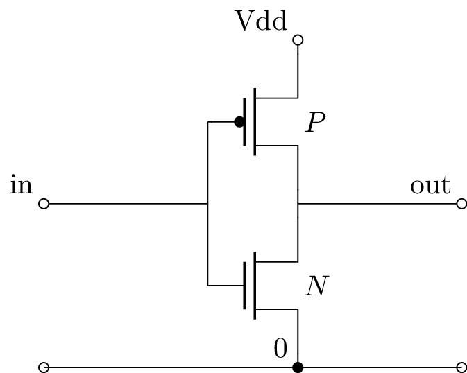
CMOS inverter
M1 3_c 2_p Vdd pmos P; right
M2 3_c 2_n 0 nmos N; right
W 2_p 2_c; down=0.5
W 2_c 2_n; down=0.5
W in 2_c; right
W 3_c out; right
P1 in 0_2; down
P2 out 0_3; down
W 0_2 0;right
W 0 0_3;right
Diode bridge
D1 1 2; left=1.5
D2 3 4; right
D3 1 4; down=1.5
D4 3 2; up

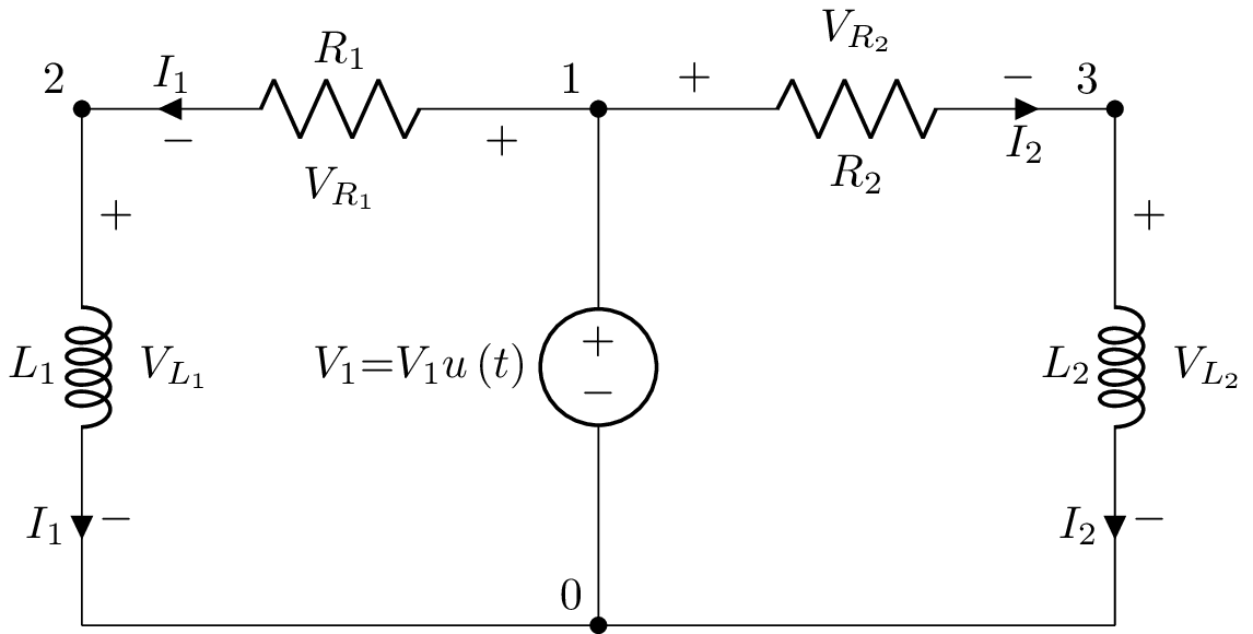
Labelled circuit
V1 1 0 step; down
R1 1 2; left=2, i=I_1, v=V_{R_1}
R2 1 3; right=2, i=I_2, v=V_{R_2}
L1 2 0_1; down=2, i=I_1, v=V_{L_1}
L2 3 0_3; down=2, i=I_2, v=V_{L_2}
W 0 0_3; right
W 0 0_1; left
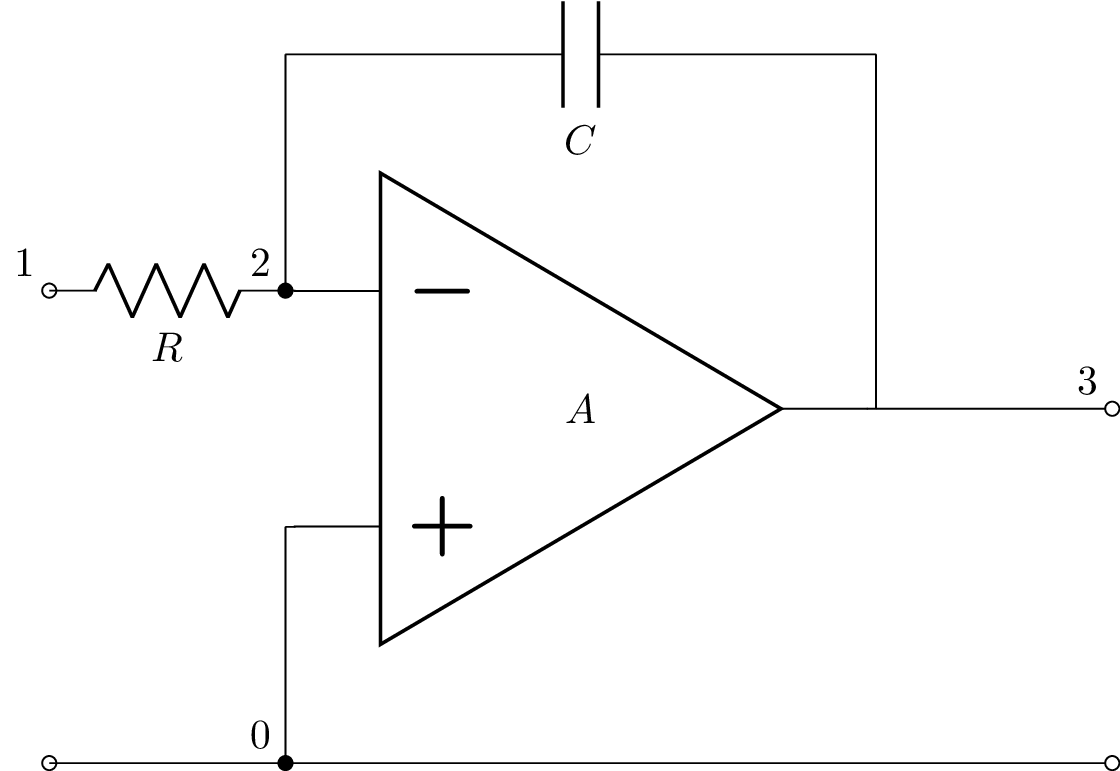
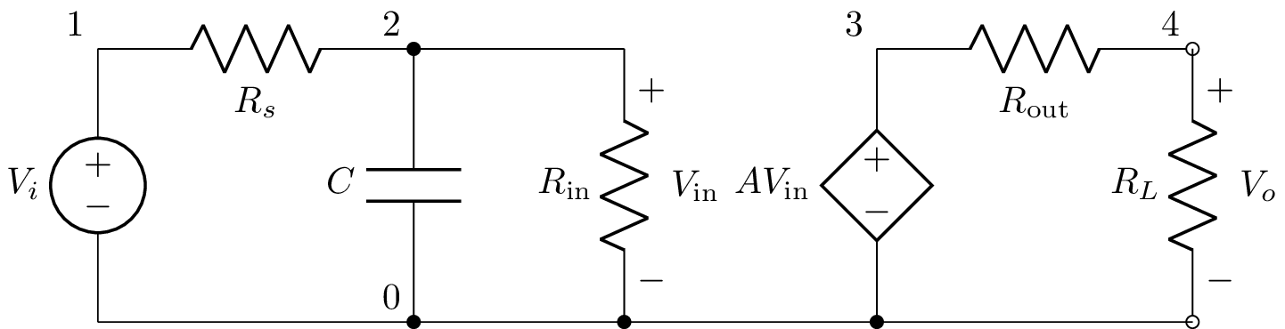
Loaded opamp model
Vi 1 0_1; down=1.3
Rs 1 2; right=1.5
C 2 0; down
W 0_1 0; right
W 0 0_2; right
Rin 2_2 0_2; down, v=V_{in}
W 2 2_2; right
E1 3 0_3 2 0 A; down, l=A V_{in}
Rout 3 4; right=1.5
RL 4 0_4; down=1.3, v=V_o
W 0_2 0_3; size=1.2
W 0_3 0_4
P1 4 0_4; down
; draw_nodes=connected
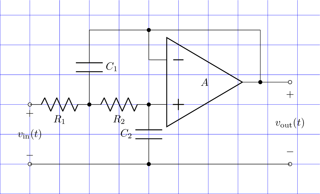
Sallen Key filter
P 1 0; down, v_=v_{in}(t)
R1 1 2; right
R2 2 3; right
C1 2 4; up
C2 3 9; down
W 4 5; right
W 5 6; right
W 6 7; down=0
W 7 8; right=0.5
E 7 0 opamp 3 11 A; right, mirror, scale=0.75, size=0.75
W 5 11; down=0.5
P 8 10; down, v^=v_{out}(t)
W 0 9; right
W 9 10; right
;draw_nodes=connections, label_nodes=False, help_lines=1
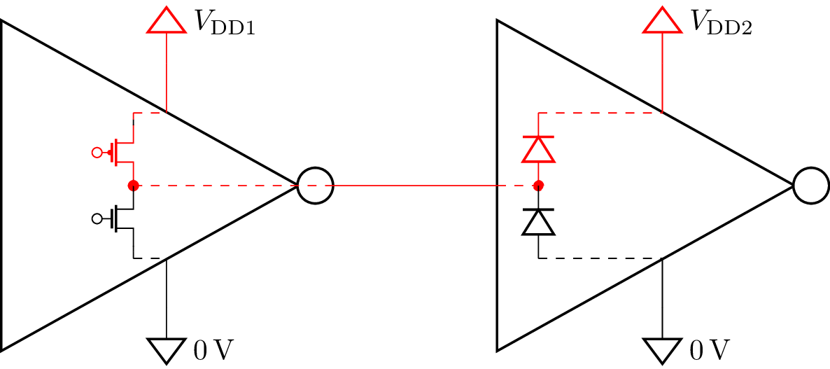
CMOS back-drive
U1 inverter; right=2, l={}
U2 inverter; right=2, l={}
W U1.out U2.in; right=1, color=red
W U1.vss 4_2; down=0.3, 0V
W U2.vss 4_3; down=0.3, 0V
W U1.vdd 3_2; up=0.3, implicit, l=V_{DD1}, color=red
W U2.vdd 3_3; up=0.3, implicit, l=V_{DD2}, color=red
W U2.in 7_1; right=0.25, dashed, fixed, color=red
D1 7_1 6_1; up=0.25, scale=0.5, l=, color=red
D2 6_2 7_1; up=0.25, scale=0.5, l=
W 6_1 U2.vdd; right=0.6, dashed, color=red
W 6_2 U2.vss; right=0.6, dashed
M1 1 2 3 pmos; right=0.4, scale=0.4, l={}, color=red
M2 1 4 5 nmos; right=0.4, scale=0.4, l={}
W 3 3_1; up=0.0, color=red
W 3_1 U1.vdd; right=0.2, dashed, color=red
W 5 5_1; down=0.0
W 5_1 U1.vss; right=0.2, dashed
W 1 U1.out; right, dashed, color=red
;draw_nodes=connections,label_nodes=false,thickness=2
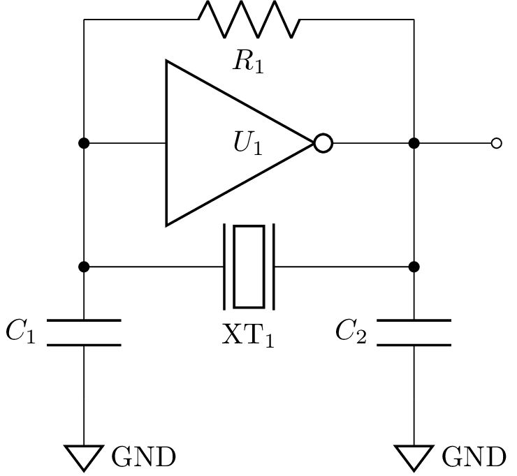
Pierce oscillator
U1 inverter; right
W 5 U1.in; right=0.5
W U1.out 6; right=0.5
W 6 9; right=0.5
R1 7 8; right
W 5 1; down=0.75
W 6 2; down=0.75
W 5 7; up=0.75
W 6 8; up=0.75
XT1 1 2; right
C1  1 4; down=0.8
C2  2 3; down=0.8
W 4 0; down=0.1, implicit, l=GND
W 3 0; down=0.1, implicit, l=GND
; draw_nodes=connections, label_nodes=False
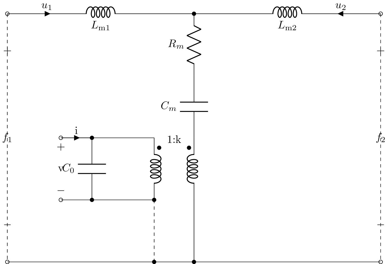
Accelerometer
In this example, a dashed wire connects the electrical and mechanical grounds for simulation.
Pm1 1 0_1; down, v=f_1
Pm2 2 0_2; down, v=f_2
Lm1 1 3; right=3, i>^=u_1
Lm2 3 2; right=3, i^<=u_2
Rm 3 4; down
Cm 4 5; down
TF 5 6 9 0 k; right
W 6 0_6; down
W 0_1 0_10; right
W 0_10 0_6; right, free
W 0_6 0_2; right

Pe 7 0_7; down, v_=v
W 7 8; right=0.75, i=i
W 0_7 0_8; right=0.75
W 8 9; right
W 0_8 0; right
C0 8 0_8; down
W 0 0_10; down, dashed
; label_nodes=none, draw_nodes=connections
Customisation
Circuitikz commands (indeed any TikZ/PGF macros) can be embedded in a netlist. Here’s an example that embeds a Circuitikz command to change the inductor style:
L1 1 2; right
;; \ctikzset{inductor=cute}
L2 2 3; right
File formats
Lcapy uses the filename extension to determine the file format to produce. This must be one of tex, schtex, pgf, png, svg, or pdf. The pgf format is useful for including schematics into LaTeX documents. The tex, schtex, and pgf extension generates a standalone LaTeX file. If no filename is specified, the schematic is displayed on the screen.
By default, the png format is used for interactive drawing. However, being a bit-mapped image, the quality is poor. First, LaTeX is used to create a temporary pdf file; this is then converted to png format. Several strategies are tried to do the conversion:
ghostscript
ImageMagick convert (By default pdf conversions are disabled. On a Linux system edit /etc/ImageMagick-6/policy.xml to enable this conversion.)
pdftoppm (this does a poor job with thin lines)
When using a Jupyter notebook, the svg format can be used with draw(svg=True). However, Jupyter has problems loading multiple svg files.
Use cct.draw(debug=2) to determine which conversion program Lcapy selects.
schtex
schtex is a Python script that will generate a schematic from a netlist file. For example, here’s how a png file can be generated:
$ schtex circuit.sch circuit.png
Similarly, a pdf file is created using:
$ schtex circuit.sch circuit.pdf
A stand-alone LaTeX file can be obtained using:
$ schtex circuit.sch circuit.tex
This can be converted to a pdf file using pdflatex.
If you wish to include the schematic into a LaTeX file use:
$ schtex circuit.sch circuit.pgf
and then include the file with \input{circuit.pgf}. The pgf format is a vector graphics format using LaTeX macros. Its advantage is that the schematic fonts match the rest of the document. To match the fonts for a pdf or png format requires some customisation. You will need to include the Circuitikz package, see Schematics in LaTeX.
schtex has many command line options to configure the drawing. These override the options specified in the netlist file. For example:
$ schtex --draw_nodes=connections --label_nodes=false --cpt-size=1 --help_lines=1 circuit.sch circuit.pdf
Installation
Note, you will need schtex to be on your path. If installing Lcapy with pip, schtex is usually installed in ~/.local/bin or /usr/local/bin.
Customisation
The drawing can be customised using the following options:
autoground: enables automatically drawing of implicit ground connections. Its argument can specify the type of connection (ground, sground, rground, etc). If the argument is False this feature is disable. If the argument is True, this feature is enabled using the the default symbol sground.
draw-nodes enables node drawing. The argument can be ‘none’, ‘connections’, ‘primary’, ‘all’.
font specifies the font (e.g., ‘\small’, ‘\sffamily\tiny’).
include inserts a string at the start of the document (this is useful to switch to different fonts).
includefile inserts the contents of a file at the start of the document (this is useful to switch to different fonts).
label-ids controls whether the component names are shown.
label-nodes controls whether the node names are shown. The argument can be ‘none’, ‘alpha’, ‘pins’, ‘primary’, ‘all’, or a list of comma separated node names in braces.
label-values controls whether the component values are shown.
label-delimiter controls the formatting of labels. The default is ‘=’. This produces something like V1=10 V. If the delimiter is ‘\’ a stacked label is created with the component name above the component value. If the delimiter is ‘_’, the component name and value are placed on opposite sides of the component.
label-flip flips the position of the label.
node-label-anchor: specifies where the node is relative to the node label (default south east).
postamble inserts a command at the end of the drawing commands.
preamble inserts a command at the start of the drawing commands.
style controls the schematic style. The argument can be ‘american’, ‘british’, or ‘european’.
voltage-dir specifies how voltage sources are annotated. The argument can be RP (for rising potential) or EF (for electric field).
The include and includefile option are only used for creating a stand-alone file. They are useful for customising the fonts to match the document they are to be embedded in.
Node renumbering
One useful schtex option is to renumber the nodes in a netlist. For example,
$ schtex --renumber='10:1, 11:2' infile.sch outfile.sch
In this case node 10 is converted to node 1 and node 11 is converted to node 2.
All the nodes can be automatically renumbered using:
$ schtex --renumber='all' infile.sch outfile.sch
This will choose small integers for the node numbers, honoring the provided mapping. Equipotential nodes will be distinguished using enumerated subscripts, e.g., 1_1, 1_2, 1_3 etc.
Schematics in LaTeX
Here’s an example of how to include an Lcapy schematic in a LaTeX document.
\documentclass[a4paper, 12pt]{article}
\usepackage{circuitikz}

\begin{document}

\begin{figure}
  \centering
  \input{pic4.pgf}
  \caption{RLC network.}
\end{figure}

\end{document}
If this file is called pic4-demo.tex, a PDF file can be produced using:
$ schtex pic4.sch pic4.pgf
$ pdflatex pic4-demo
Drawing tips
The fastest way to generate a schematic is to draw a rough sketch, enumerate the nodes, and then enter a netlist. To reduce confusion if this is an error, test it as you go, say using the schtex program.
Lcapy uses a semi-automated approach to component layout. For each component it needs its orientation and size. By default the size is 1. This is the minimum distance between its nodes (for a one-port device). If the component can be stretched, Lcapy will increase but never decrease this distance.
The x and y positions of nodes are computed independently using a graph algorithm. An error can occur if components have the wrong orientation since this makes the graph inconsistent. Unfortunately, it is not trivial to find the offending component so it is best to draw a schematic incrementally and to test it as you go.
Problems can occur using components, such as integrated circuits and opamps, that cannot be stretched. Usually this is due to a conflict between constraints. A solution is to reduce the size of the component if it can be stretched, such as a wire or resistor. Sometimes it is necessary to add a short interconnecting wire.
The stretching of components can be prevented by specifying the fixed attribute.
Additional constraints can be supplied by using an open-circuit to align components.
Grid lines can be added to a schematic using some Tikz markup. For example:
;;\draw[help lines] (0,0) grid [xstep=0.1, ystep=0.1] (10,5);
By default, for circuit analysis, the primary circuit nodes are shown and labelled. However, for a schematic it is best to only show the nodes where components are connected; this can be achieved with:
;;draw_nodes=connections
The node labels can be removed with:
;;label_nodes=none
The drawing quality depends on the installed version of Circuitikz due to slight tweakings of component sizes.
Problems
Circuitikz is a moving target and the components are often tweaked. This causes slight alignment problems. Please submit an issue (see Issue reporting).
Circuitikz does not correctly determine the bounding box for transistor text labels. A workaround is to draw a dummy component to extend the bounding box.
If the circuit is not drawn, use cct.draw(debug=2) to see what fails.
To determine the version of Circuitikz, use cct.draw(debug=1).